Academic Profile
Statistics
Similar Authors
Papers on arXiv
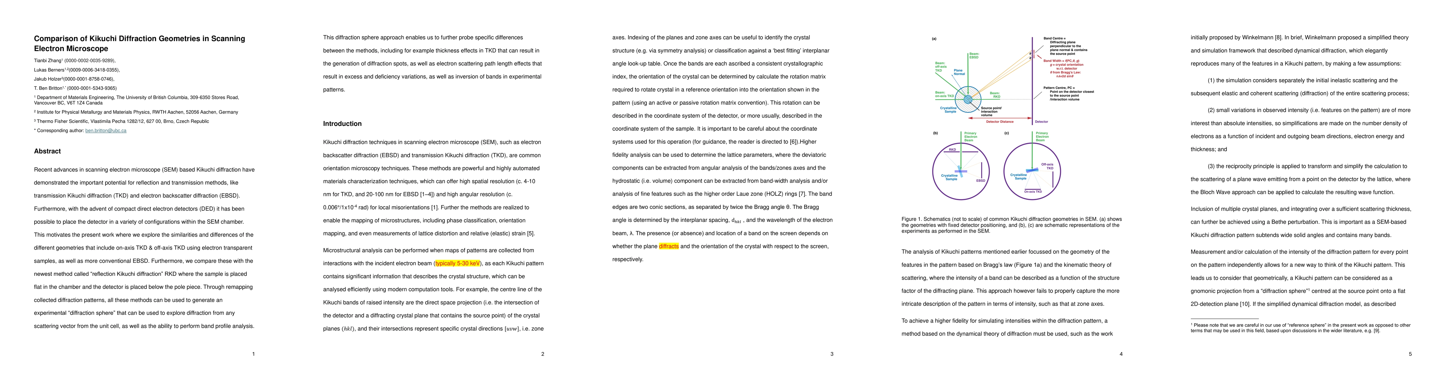
To engineer the next generation of advanced materials we must understand their microstructure, and this requires microstructural characterization. This can be achieved through the collection of high...
Diffraction pattern analysis can be used to reveal the crystalline structure of materials, and this information is used to nano- and micro-structure of advanced engineering materials that enable mod...
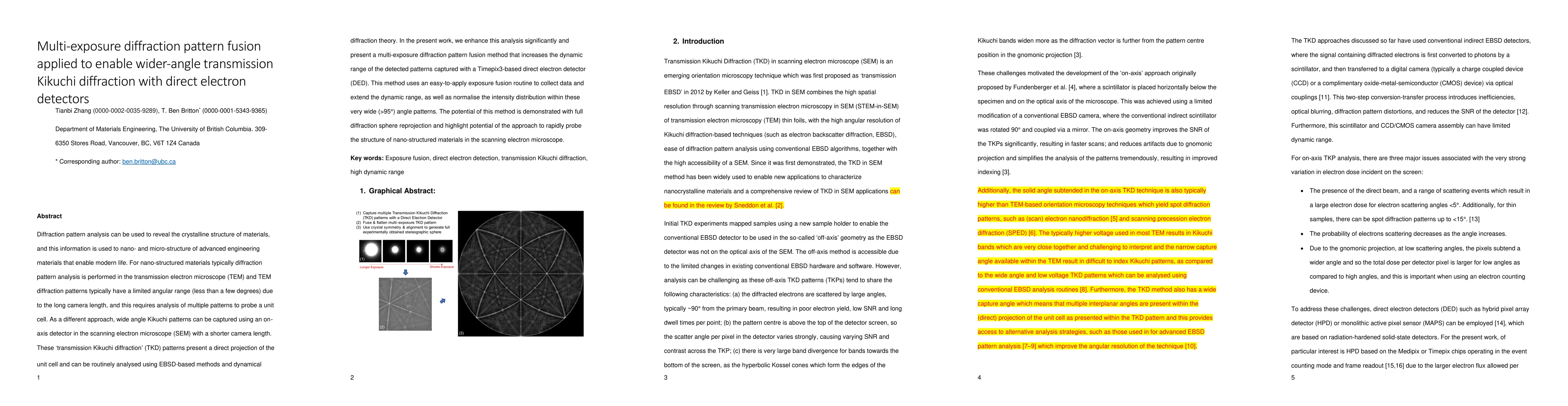
Recent advances in scanning electron microscope (SEM) based Kikuchi diffraction have demonstrated the important potential for reflection and transmission methods, like transmission Kikuchi diffraction...
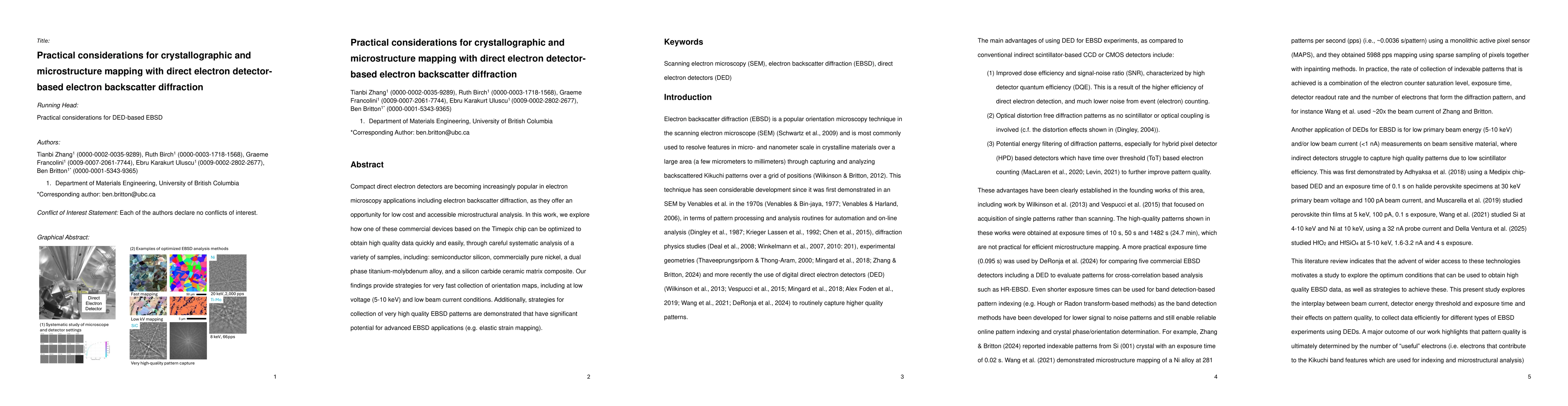
Compact direct electron detectors are becoming increasingly popular in electron microscopy applications including electron backscatter diffraction, as they offer an opportunity for low cost and access...
Electron channeling contrast imaging (ECCI) is a scanning electron microscopy (SEM) based technique that enables bulk-sample characterization of crystallographic defects (e.g. dislocations, stacking f...
The study of thin films and 2D materials, including transition metal dichalcogenides such as WSe$_2$ offers opportunities to leverage their properties in advanced sensors, quantum technologies, and de...
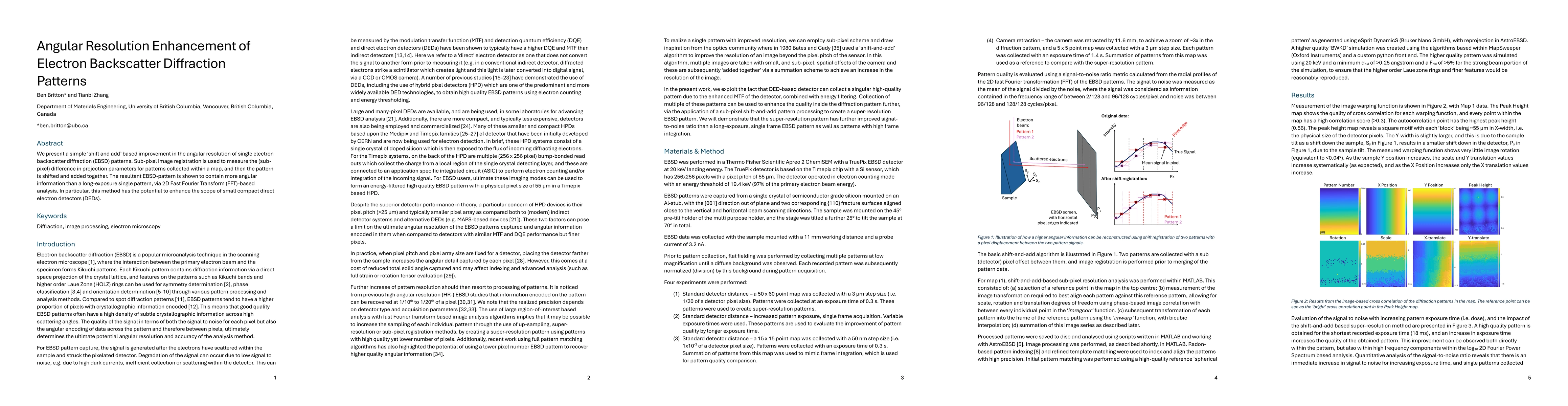
We present a simple 'shift-and-add' based improvement in the angular resolution of single electron backscatter diffraction (EBSD) patterns. Sub-pixel image registration is used to measure the (sub-pix...
Transmission Kikuchi diffraction in the scanning electron microscope has gained popularity as a materials characterization technique for its high throughput and nanometer-level spatial resolution. Whi...