Publication
Metrics
AI Quick Summary
This paper introduces a multi-exposure diffraction pattern fusion technique to enhance transmission Kikuchi diffraction (TKD) analysis in SEMs, enabling wider-angle data collection with direct electron detectors. This method extends the dynamic range and normalizes the intensity distribution, allowing for comprehensive unit cell analysis of nano-structured materials.
Paper Preview
Abstract
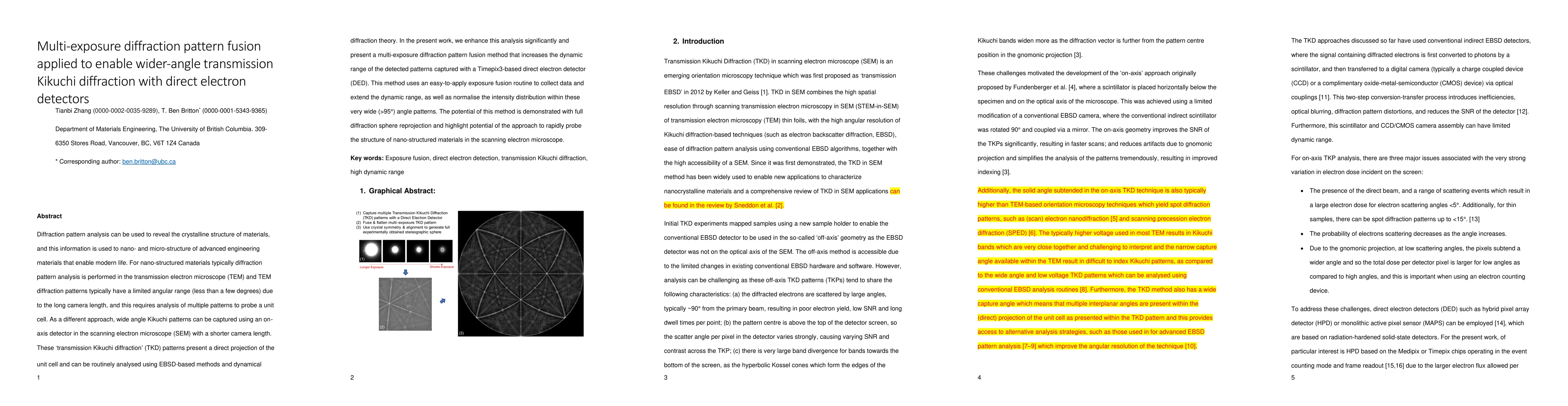
Diffraction pattern analysis can be used to reveal the crystalline structure of materials, and this information is used to nano- and micro-structure of advanced engineering materials that enable modern life. For nano-structured materials typically diffraction pattern analysis is performed in the transmission electron microscope (TEM) and TEM diffraction patterns typically have a limited angular range (less than a few degrees) due to the long camera length, and this requires analysis of multiple patterns to probe a unit cell. As a different approach, wide angle Kikuchi patterns can be captured using an on-axis detector in the scanning electron microscope (SEM) with a shorter camera length. These 'transmission Kikuchi diffraction' (TKD) patterns present a direct projection of the unit cell and can be routinely analyzed using EBSD-based methods and dynamical diffraction theory. In the present work, we enhance this analysis significantly and present a multi-exposure diffraction pattern fusion method that increases the dynamic range of the detected patterns captured with a Timepix3-based direct electron detector (DED). This method uses an easy-to-apply exposure fusion routine to collect data and extend the dynamic range, as well as normalize the intensity distribution within these very wide (>95{\deg}) angle patterns. The potential of this method is demonstrated with full diffraction sphere reprojection and highlight potential of the approach to rapidly probe the structure of nano-structured materials in the scanning electron microscope.
AI Key Findings
Get AI-generated insights about this paper's methodology, results, significance, and more — seven facets brought into focus.
Impact
Paper Details
Authors
PDF Preview
Key Terms
Citation Network
Current paper (gray), citations (green), references (blue)
Display is limited for performance on very large graphs.
Discussion 0