Academic Profile
Statistics
Similar Authors
Papers on arXiv
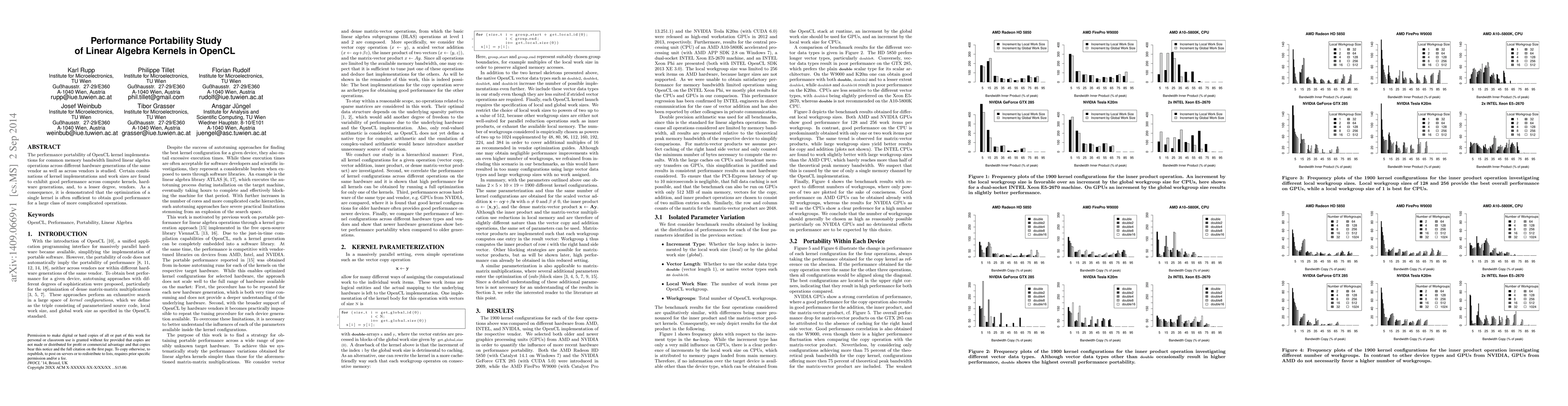
The performance portability of OpenCL kernel implementations for common memory bandwidth limited linear algebra operations across different hardware generations of the same vendor as well as across ...
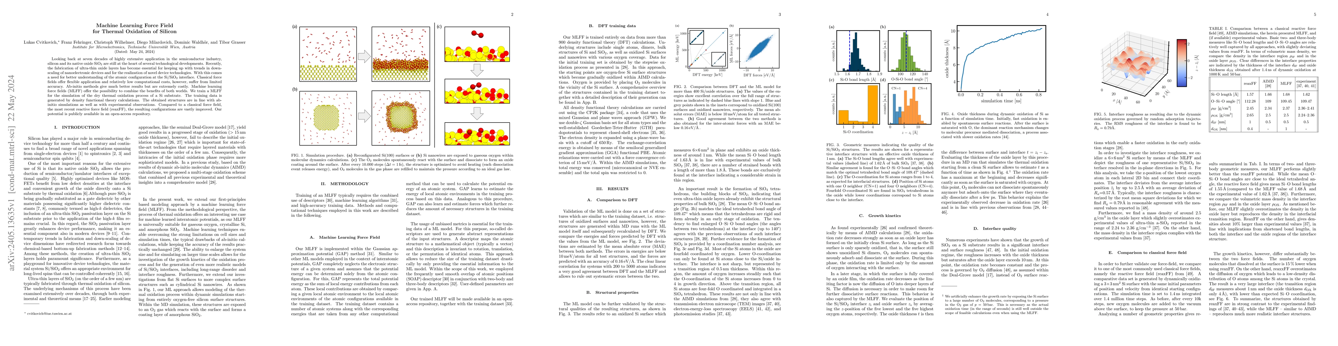
Looking back at seven decades of highly extensive application in the semiconductor industry, silicon and its native oxide SiO$_2$ are still at the heart of several technological developments. Recent...
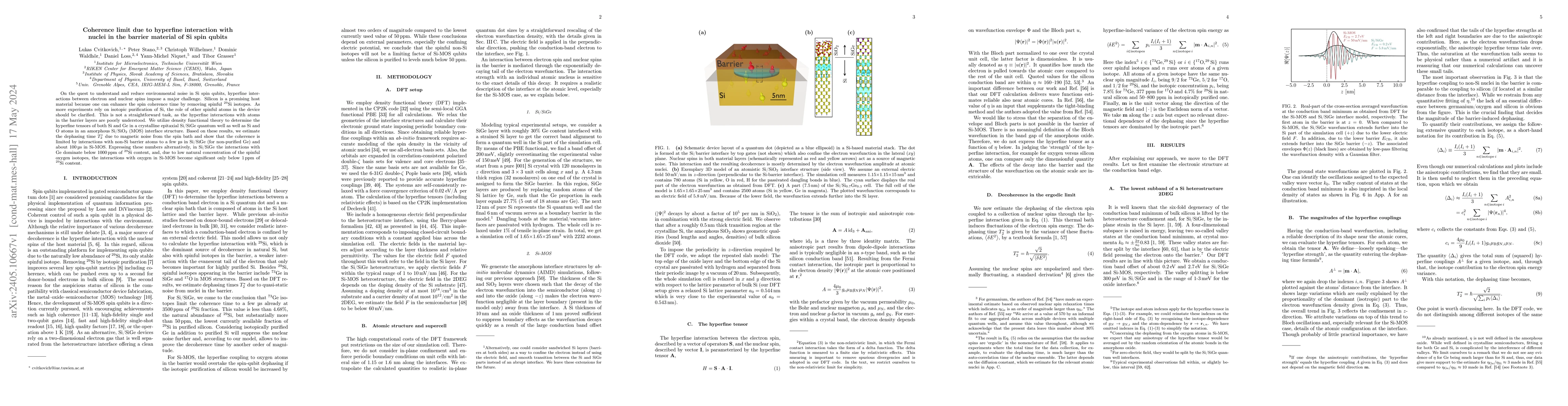
On the quest to understand and reduce environmental noise in Si spin qubits, hyperfine interactions between electron and nuclear spins impose a major challenge. Silicon is a promising host material ...
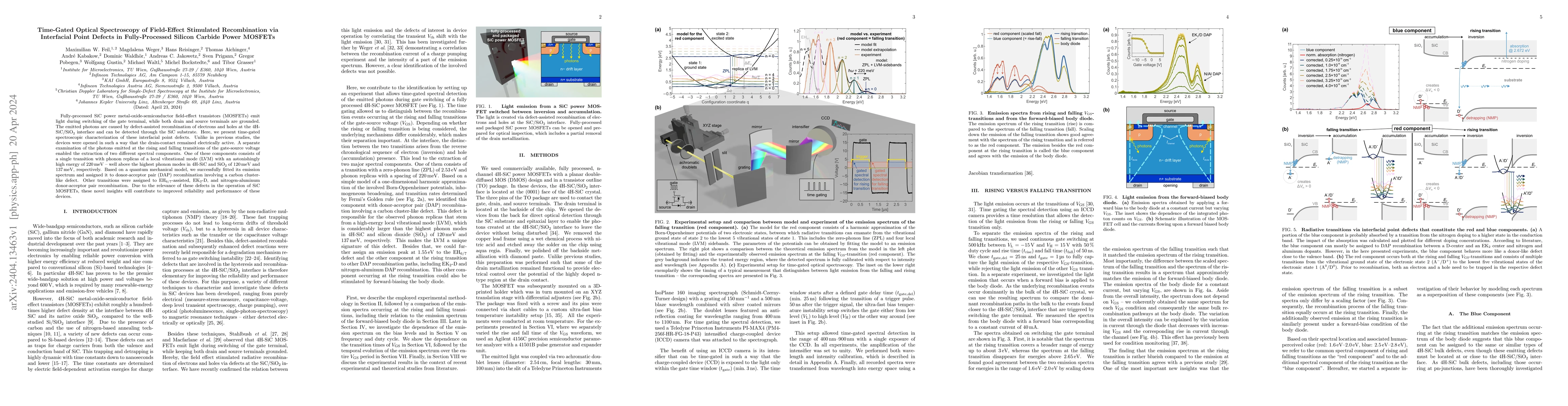
Fully-processed SiC power metal-oxide-semiconductor field-effect transistors (MOSFETs) emit light during switching of the gate terminal, while both drain and source terminals are grounded. The emitt...
Graphene is a promising material for applications as a channel in graphene field-effect transistors (GFETs) which may be used as a building block for optoelectronics, high-frequency devices and sens...
Charge trapping plays an important role for the reliability of electronic devices and manifests itself in various phenomena like bias temperature instability (BTI), random telegraph noise (RTN), hys...
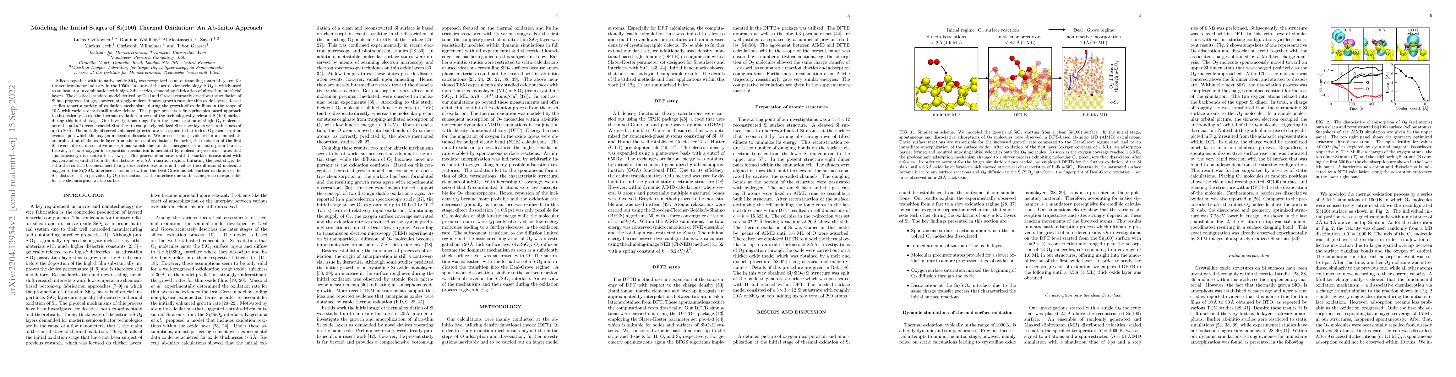
Silicon together with its native oxide SiO$_2$ was recognized as an outstanding material system for the semiconductor industry in the 1950s. In state-of-the-art device technology, SiO$_2$ is widely ...
Silicene is one of the most promising 2D materials for the realization of next-generation electronic devices, owing to its high carrier mobility and bandgap tunability through the imposition of an e...
Despite the enormous progress achieved during the past decade, nanoelectronic devices based on two-dimensional (2D) semiconductors still suffer from a limited electrical stability. This limited stab...
Complementary metal oxide semiconductor (CMOS) logic circuits at the ultimate scaling limit place the utmost demands on the properties of all materials involved. The requirements for semiconductors ...
The recent progress in nanosheet transistors has established two-dimensional (2D) semiconductors as viable candidates for future ultra-scaled electronic devices. Next to reducing contact resistance, i...
Continued miniaturization of transistors is critical for sustaining advances in computing performance, energy efficiency, and integration density. A central nanoscale challenge is controlling gate lea...
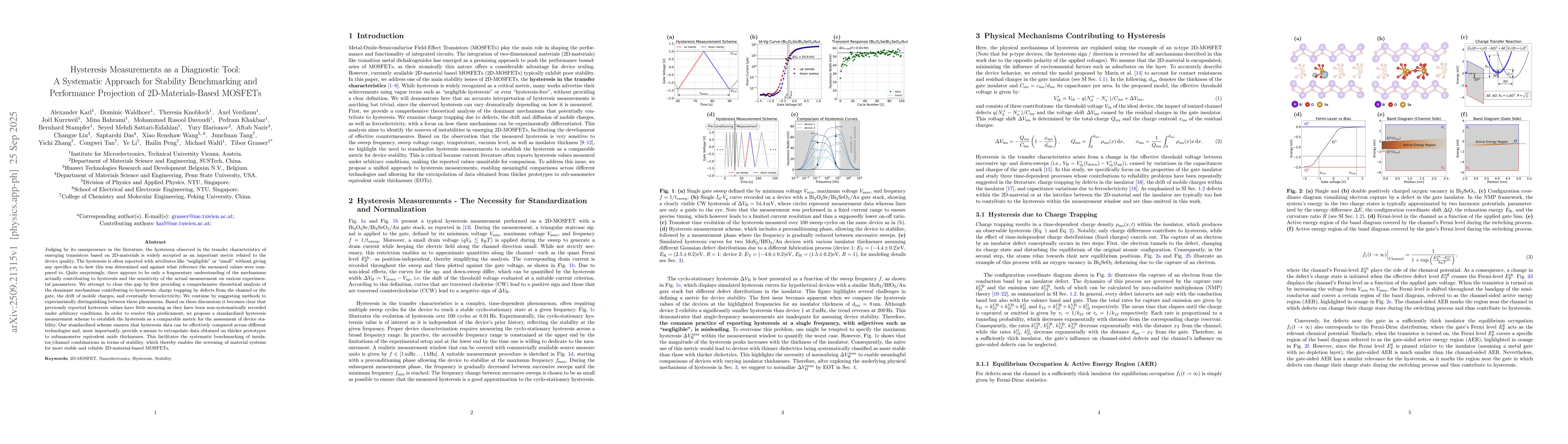
Judging by its omnipresence in the literature, the hysteresis observed in the transfer characteristics of emerging transistors based on 2D-materials is widely accepted as an important metric related t...
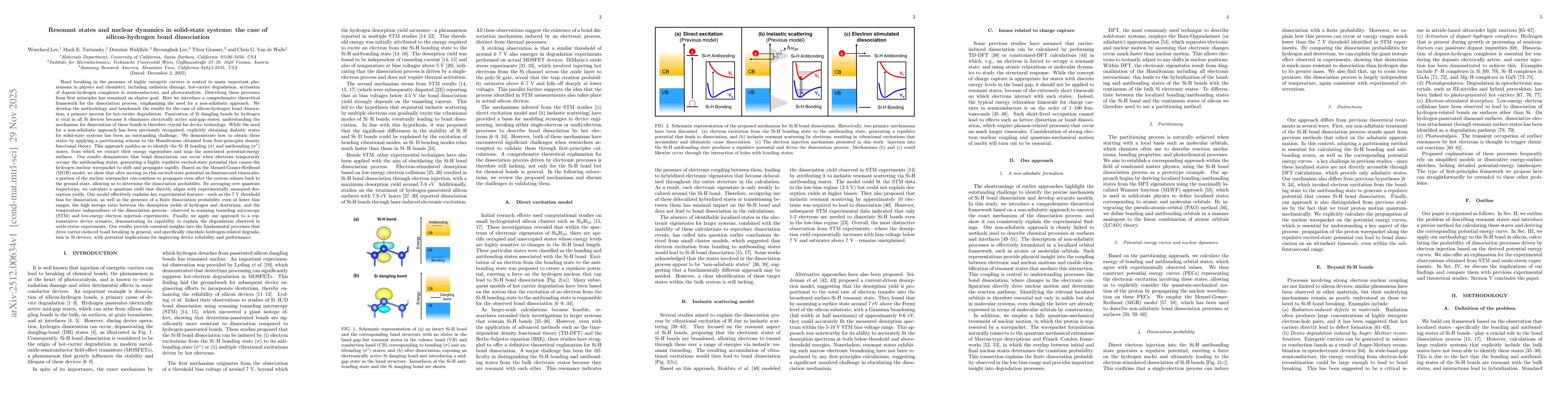
Bond breaking in the presence of highly energetic carriers is central to many important phenomena in physics and chemistry, including radiation damage, hot-carrier degradation, activation of dopant-hy...
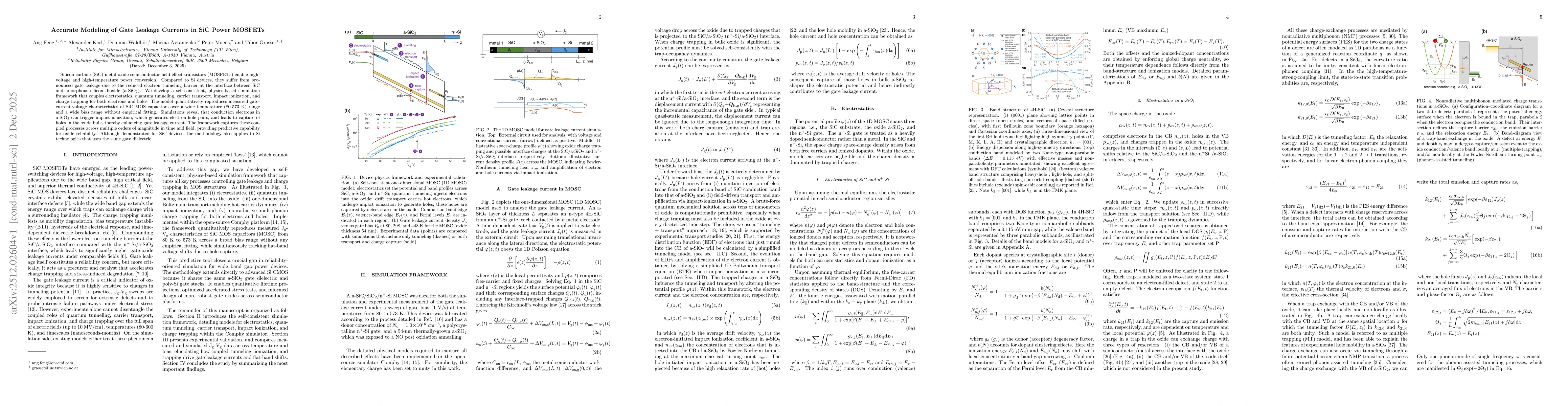
Silicon carbide (SiC) metal-oxide-semiconductor field-effect-transistors (MOSFETs) enable high-voltage and high-temperature power conversion. Compared to Si devices, they suffer from pronounced gate l...
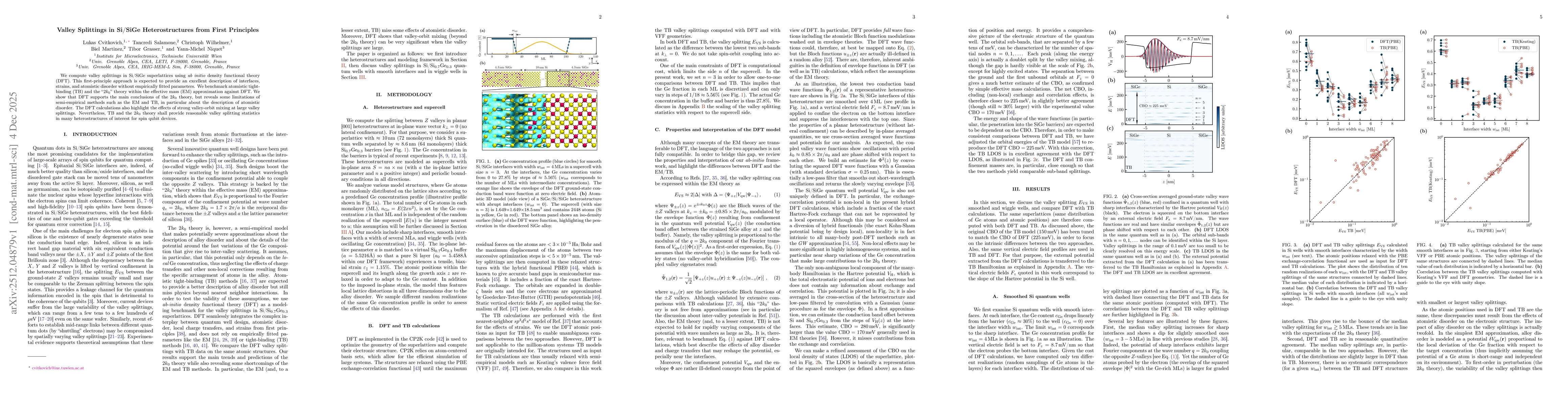
We compute valley splittings in Si/SiGe superlattices using ab initio density functional theory (DFT). This first-principle approach is expected to provide an excellent description of interfaces, stra...
While 2D materials have enormous potential for future device technologies, many challenges must be overcome before they can be deployed at an industrial scale. One of these challenges is identifying t...