ArxivLens
ArXiv cond-mat.mes-hall

The van der Waals Gap: a Hidden Showstopper in Semiconductor Device Scaling

Mahdi Pourfath, Tibor Grasser

2509.17617 Published Sep 22, 2025
View PDF

Publication

Published: Sep 22, 2025
Categories: cond-mat.mes-hall

Metrics

Source: ArXiv

Quick Answers

What methodology did the authors use?

The research employs a combination of quantum transport modeling, complex band structure analysis, and electrostatic scaling principles to evaluate gate leakage current in metal-insulator-semiconductor structures. It incorporates dead-layer effects and van der Waals (vdW) gap considerations through effective permittivity models and transmission probability calculations. More in Methodology →

What are the key results?

The study identifies that dead-layer effects significantly reduce the effective permittivity of high-κ dielectrics like SrTiO3 in ultrathin films, limiting their scaling benefits. — The two-band Franz model provides accurate predictions of tunneling current decay rates across wide-gap insulators by accounting for both conduction and valence band contributions. More in Key Results →

Why is this work significant?

This research advances the understanding of gate leakage mechanisms in advanced semiconductor devices, providing critical insights for optimizing dielectric materials and gate stack designs in sub-10nm technologies. The findings are crucial for achieving energy-efficient, high-performance integrated circuits. More in Significance →

What are the main limitations?

The simplified two-band model may not capture all quantum mechanical effects in complex band structures. — The analysis assumes idealized conditions that may not fully represent real-world device variations and manufacturing tolerances. More in Limitations →

Paper Preview

Abstract

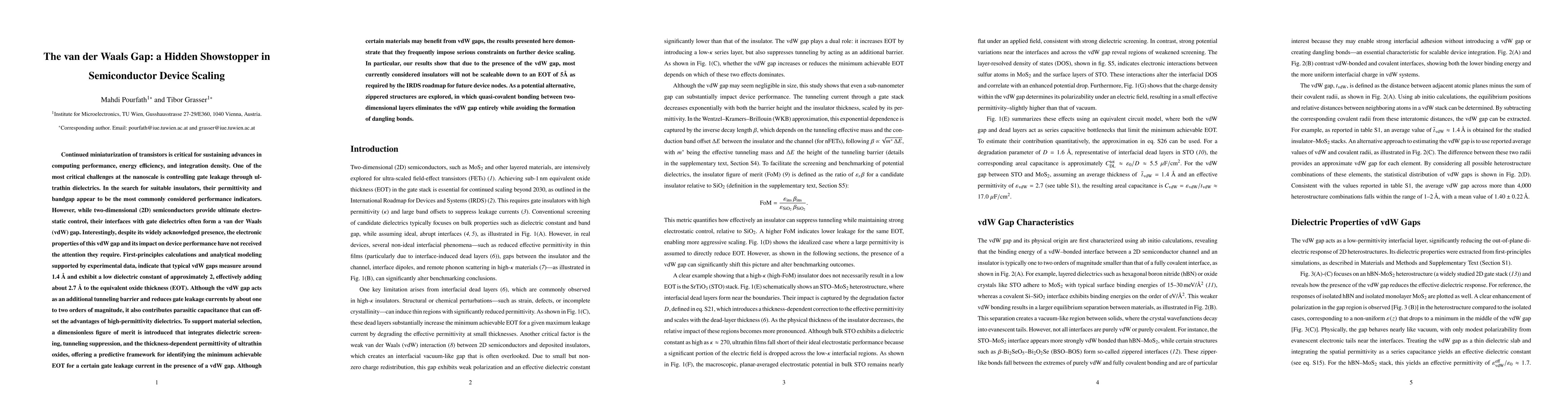
Continued miniaturization of transistors is critical for sustaining advances in computing performance, energy efficiency, and integration density. A central nanoscale challenge is controlling gate leakage through ultrathin dielectrics. In evaluating candidate insulators, permittivity and bandgap are often emphasized; however, interfaces between two-dimensional (2D) semiconductors and gate dielectrics typically form a van der Waals (vdW) gap whose electronic properties are underappreciated. Using first-principles calculations and analytical modeling supported by experiment, we find typical vdW gaps of about 1.4 \AA{} with an effective dielectric constant near 2, which adds roughly 2.7 \AA{} to the equivalent oxide thickness (EOT). The vdW gap serves as an additional tunneling barrier that can reduce gate leakage by one to two orders of magnitude, but it also introduces parasitic capacitance that can offset the benefits of high-k dielectrics. We introduce a dimensionless figure of merit that combines dielectric screening, tunneling suppression, and thickness-dependent permittivity of ultrathin oxides to predict the minimum achievable EOT for a target gate-leakage current in the presence of a vdW gap. Although some materials may benefit from vdW gaps, our results indicate they often impose severe constraints on further scaling. In particular, due to the vdW gap, most currently considered insulators are unlikely to scale to an EOT of 5 \AA{} as targeted by the IRDS roadmap for future nodes. As a potential alternative, we examine ``zippered'' structures in which quasi-covalent bonding between 2D layers eliminates the vdW gap while avoiding dangling bonds.
Key Findings, in focus

Seven facets of this paper, analysed and brought into focus by AI.

AI-generated · verify against source Generated Sep 29, 2025
In focus · one-line synthesis

This research advances the understanding of gate leakage mechanisms in advanced semiconductor devices, providing critical insights for optimizing dielectric materials and gate stack designs in sub-10nm technologies.

01
MethodologyHow they did it

The research employs a combination of quantum transport modeling, complex band structure analysis, and electrostatic scaling principles to evaluate gate leakage current in metal-insulator-semiconductor structures. It incorporates dead-layer effects and van der Waals (vdW) gap considerations through effective permittivity models and transmission probability calculations.

02
ResultsWhat they found
  • The study identifies that dead-layer effects significantly reduce the effective permittivity of high-κ dielectrics like SrTiO3 in ultrathin films, limiting their scaling benefits.
  • The two-band Franz model provides accurate predictions of tunneling current decay rates across wide-gap insulators by accounting for both conduction and valence band contributions.
  • Incorporating vdW gap effects into the electrostatic scaling framework reveals that tunneling through these gaps can be modeled as vacuum tunneling, consistent with DFT results.
03
SignificanceWhy it matters

This research advances the understanding of gate leakage mechanisms in advanced semiconductor devices, providing critical insights for optimizing dielectric materials and gate stack designs in sub-10nm technologies. The findings are crucial for achieving energy-efficient, high-performance integrated circuits.

04
Technical ContributionsWhat's new technically

The work introduces a unified framework that integrates electrostatic scaling, quantum tunneling models, and dead-layer effects to predict and optimize gate leakage current in advanced CMOS technologies.

05
NoveltyWhat sets it apart

This study uniquely combines van der Waals gap modeling with traditional dielectric scaling analysis, offering a comprehensive approach to understanding and mitigating gate leakage in next-generation semiconductor devices.

06
LimitationsWhat to be cautious about
  • The simplified two-band model may not capture all quantum mechanical effects in complex band structures.
  • The analysis assumes idealized conditions that may not fully represent real-world device variations and manufacturing tolerances.
07
Future WorkWhere it goes next
  • Developing more sophisticated band structure models that include multiple bands and non-parabolic dispersion relations.
  • Experimental validation of dead-layer effects in real device architectures to refine theoretical models.
  • Investigating the impact of interface states and defect densities on tunneling characteristics in high-κ dielectrics.

Paper Details

Paper ID: 2509.17617
Categories:
cond-mat.mes-hall

How to Cite This Paper

Reference manager: RIS EndNote


Discussion 0

This website uses cookies to ensure you get the best experience. Learn more