Academic Profile
Statistics
Similar Authors
Papers on arXiv
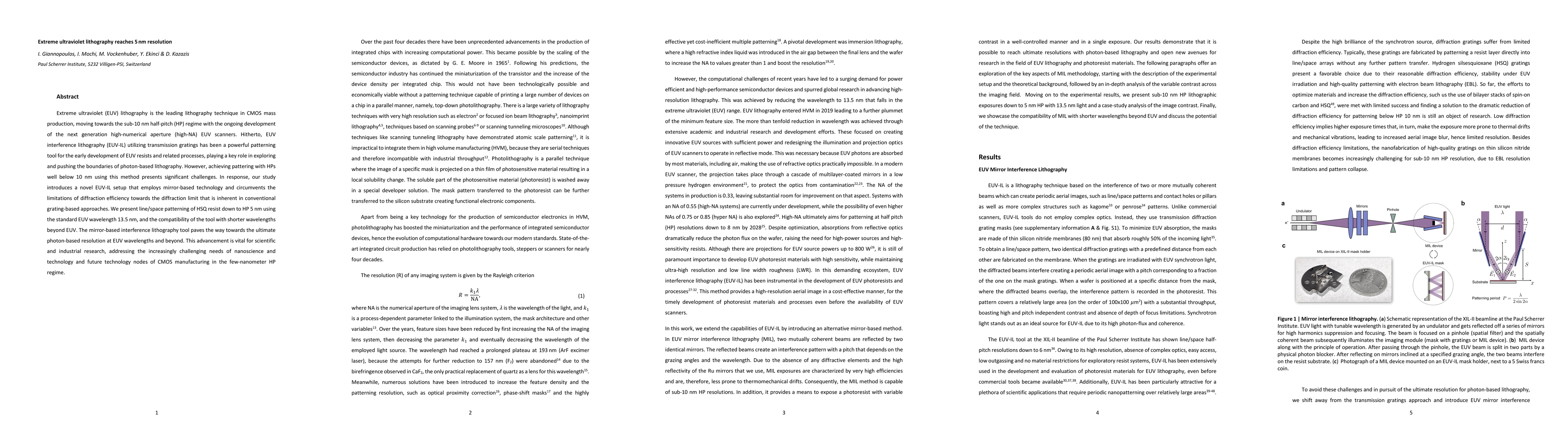
Extreme ultraviolet (EUV) lithography is the leading lithography technique in CMOS mass production, moving towards the sub-10 nm half-pitch (HP) regime with the ongoing development of the next gener...
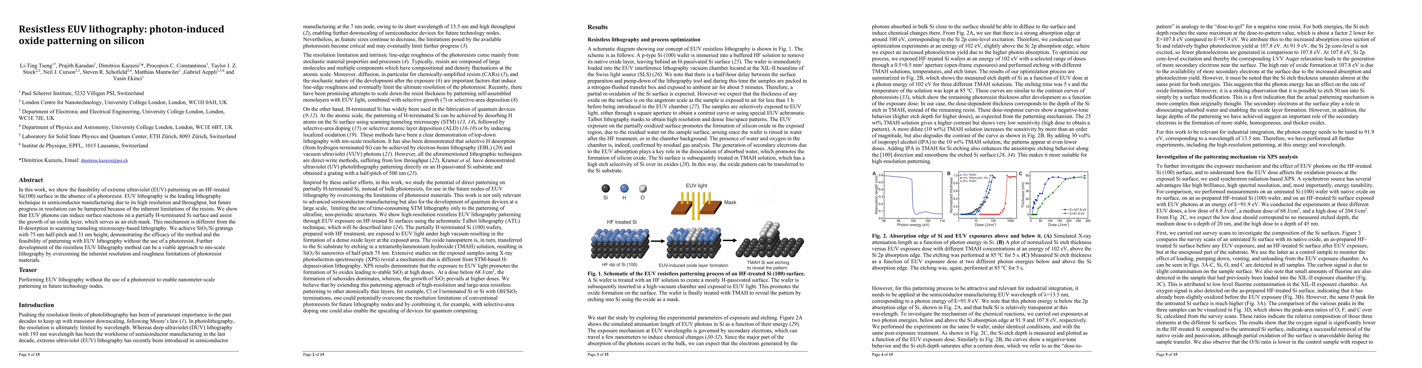
In this work, we show the feasibility of extreme ultraviolet (EUV) patterning on an HF-treated Si(100) surface in the absence of a photoresist. EUV lithography is the leading lithography technique i...
Non-volatile magnetic storage, from 1940s magnetic core to present day racetrack memory and magnetic anisotropy switching devices rely on the metastability of magnetic domains to store information. ...
High-resolution patterning of periodic structures over large areas has several applications in science and technology. One such method, based on the long-known Talbot effect observed with diffractio...
Pattern transfer by deep anisotropic etch is a well-established technique for fabrication of nanoscale devices and structures. For this technique to be effective, the resist material plays a key rol...
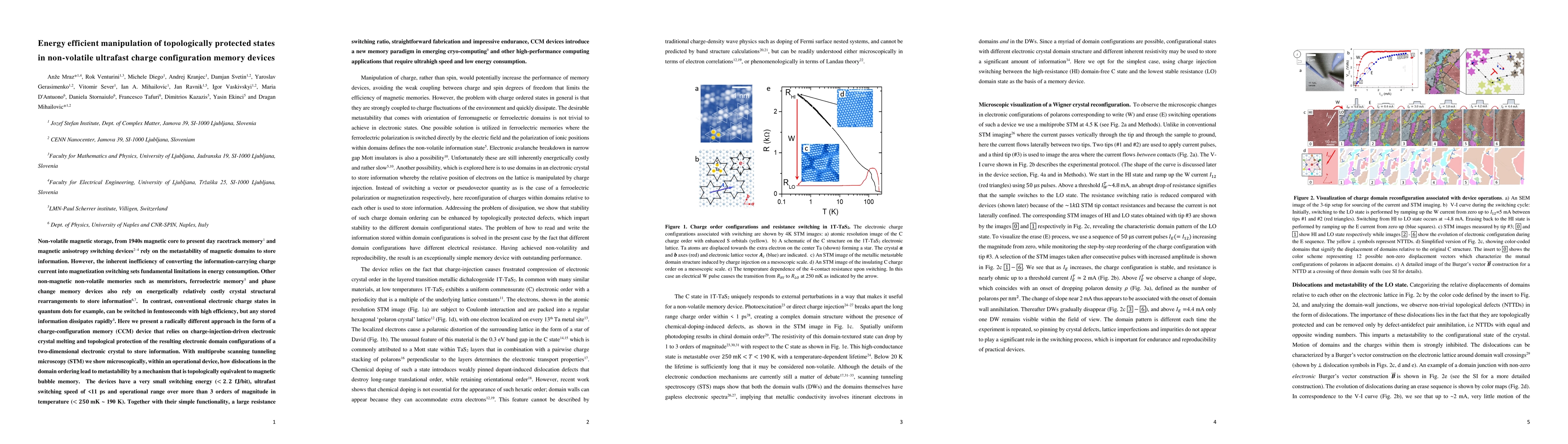
In transition metal dichalcogenides a plethora of emergent states arise from competing electron-electron and electron-phonon interactions. Among these, the non-volatile metallic 'hidden' state of 1T-T...
Spin states in semiconductors provide exceptionally stable and noise-resistant environments for qubits, positioning them as optimal candidates for reliable quantum computing technologies. The proposal...
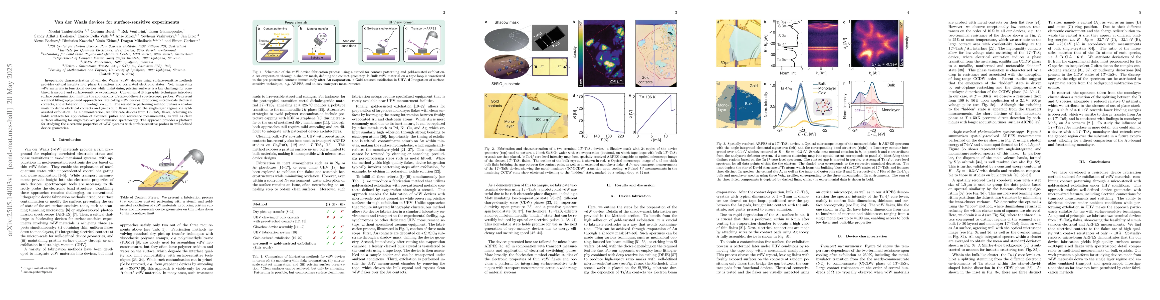
In-operando characterization of van der Waals (vdW) devices using surface-sensitive methods provides critical insights into phase transitions and correlated electronic states. Yet, integrating vdW mat...
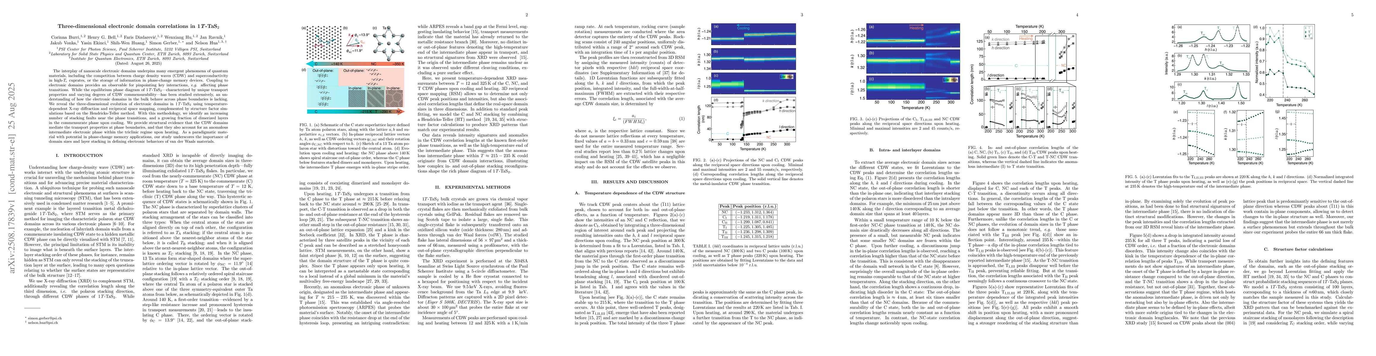
The interplay of nanoscale electronic domains underpins many emergent phenomena of quantum materials, including the competition between charge density waves (CDW) and superconductivity in high-Tc cupr...
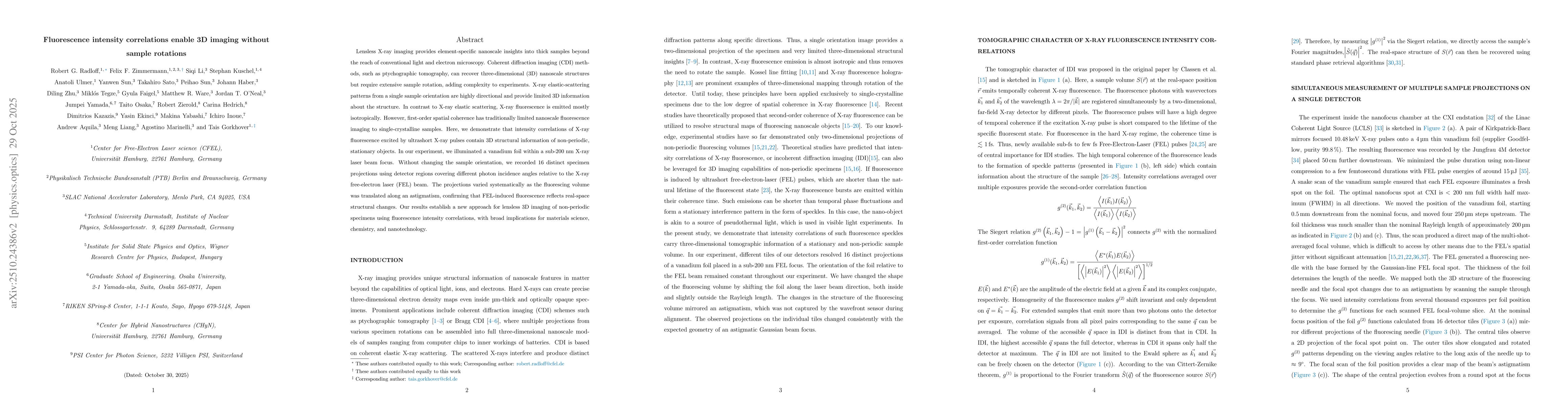
Lensless X-ray imaging provides element-specific nanoscale insights into thick samples beyond the reach of conventional light and electron microscopy. Coherent diffraction imaging (CDI) methods, such ...
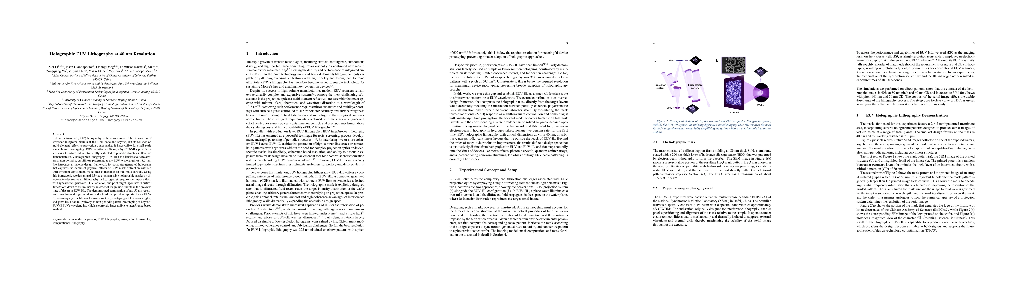
Extreme ultraviolet (EUV) lithography is the cornerstone of the fabrication of advanced integrated circuits at the 7-nm node and beyond, but its reliance on multi-element reflective projection optics ...