Publication
Metrics
AI Quick Summary
This paper introduces a novel mirror-based extreme ultraviolet interference lithography setup that achieves 5 nm half-pitch patterning, surpassing the limitations of conventional grating-based methods. The new approach enables high resolution in the sub-10 nm regime, crucial for advancing nanoscience and future CMOS manufacturing.
Paper Preview
Abstract
Extreme ultraviolet (EUV) lithography is the leading lithography technique in CMOS mass production, moving towards the sub-10 nm half-pitch (HP) regime with the ongoing development of the next generation high-numerical aperture (high-NA) EUV scanners. Hitherto, EUV interference lithography (EUV-IL) utilizing transmission gratings has been a powerful patterning tool for the early development of EUV resists and related processes, playing a key role in exploring and pushing the boundaries of photon-based lithography. However, achieving pattering with HPs well below 10 nm using this method presents significant challenges. In response, our study introduces a novel EUV-IL setup that employs mirror-based technology and circumvents the limitations of diffraction efficiency towards the diffraction limit that is inherent in conventional grating-based approaches. We present line/space patterning of HSQ resist down to HP 5 nm using the standard EUV wavelength 13.5 nm, and the compatibility of the tool with shorter wavelengths beyond EUV. The mirror-based interference lithography tool paves the way towards the ultimate photon-based resolution at EUV wavelengths and beyond. This advancement is vital for scientific and industrial research, addressing the increasingly challenging needs of nanoscience and technology and future technology nodes of CMOS manufacturing in the few-nanometer HP regime.
AI Key Findings
Get AI-generated insights about this paper's methodology, results, significance, and more — seven facets brought into focus.
Impact
Paper Details
Authors
PDF Preview
Key Terms
Citation Network
Current paper (gray), citations (green), references (blue)
Display is limited for performance on very large graphs.
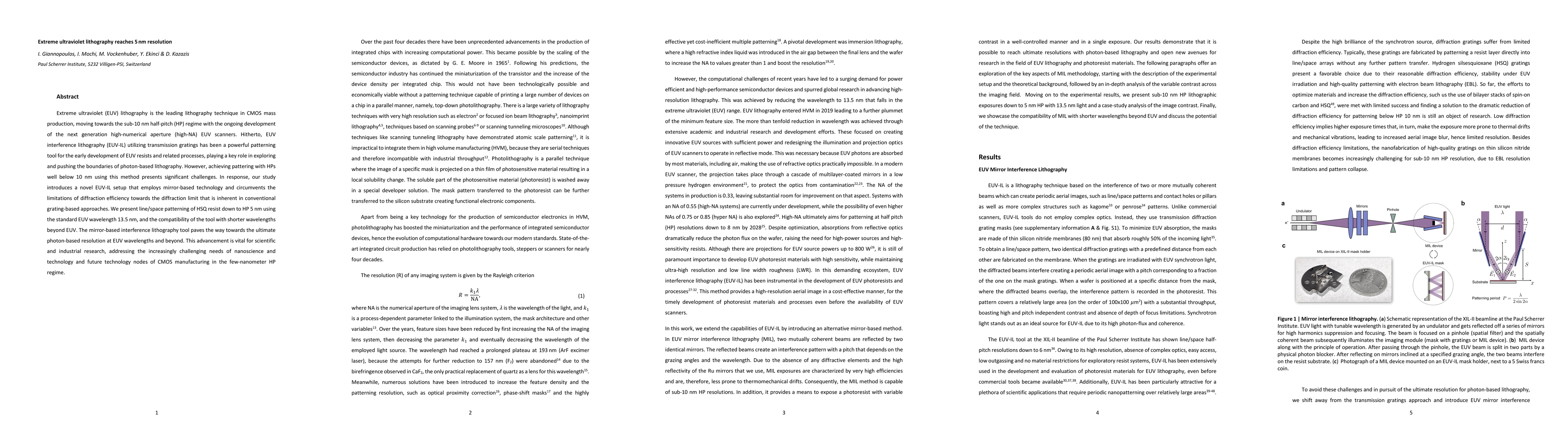
Discussion 0