2
arXiv Papers
4
Total Publications
Profile
Academic Profile
Metrics
Statistics
2
arXiv Papers
4
Total Publications
Network
Similar Authors
Publications
Papers on arXiv
arXiv
Plasmon-Driven Hot Electron Transfer at Atomically Sharp
Metal-Semiconductor Nanojunctions
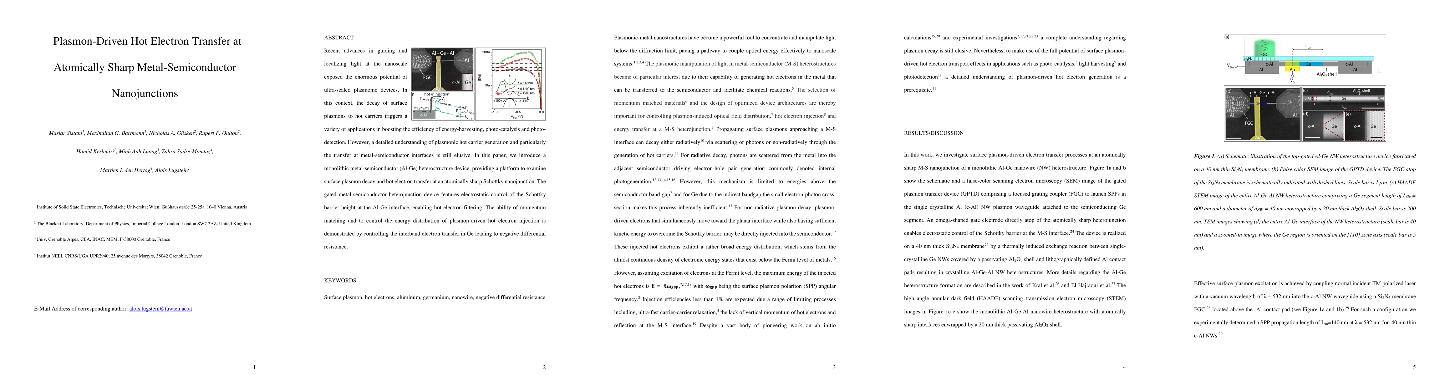
Recent advances in guiding and localizing light at the nanoscale exposed the enormous potential of ultra-scaled plasmonic devices. In this context, the decay of surface plasmons to hot carriers trig...
arXiv
Correlated and in-situ electrical transmission electron microscopy
studies and related membrane fabrication
Understanding the interplay between the structure, composition and opto-electronic properties of semiconductor nano-objects requires combining transmission electron microscopy (TEM) based techniques...