ArxivLens
Z
Researcher

Zakhar D. Kovalyuk

6 papers on arXiv

6 arXiv Papers
4 Total Publications
Profile

Academic Profile

Name Z. D. Kovalyuk
Total Papers 4
Scholar Profile View on Semantic Scholar
Metrics

Statistics

6 arXiv Papers
4 Total Publications
Publications

Papers on arXiv

Thumbnail for Terahertz control of photoluminescence emission in few-layer InSe
arXiv
Terahertz control of photoluminescence emission in few-layer InSe

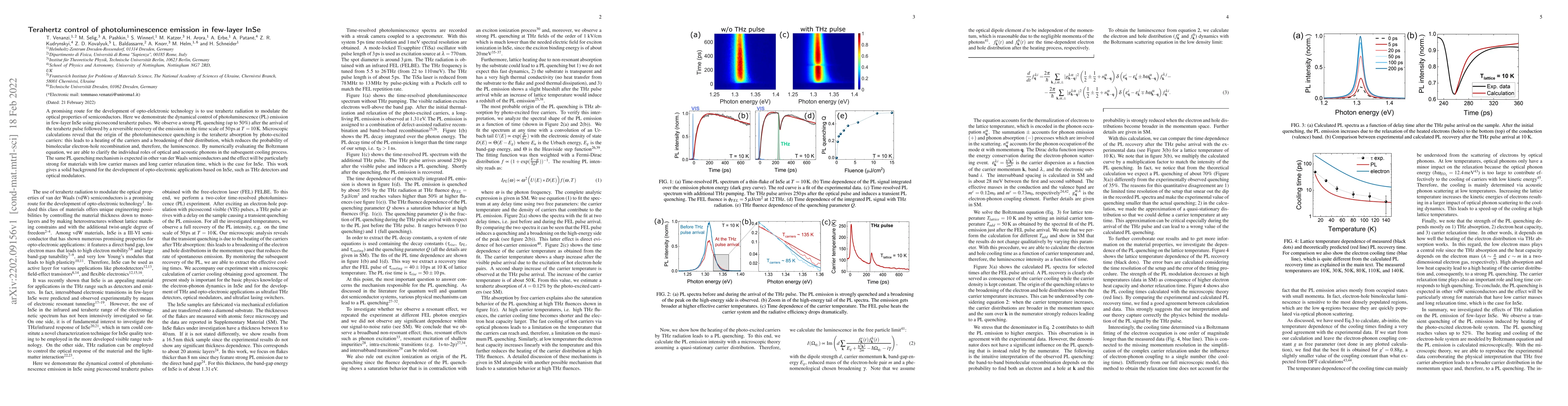
A promising route for the development of opto-elelctronic technology is to use terahertz radiation to modulate the optical properties of semiconductors. Here we demonstrate the dynamical control of ...

Thumbnail for Photoluminescence dynamics in few-layer InSe
arXiv
Photoluminescence dynamics in few-layer InSe

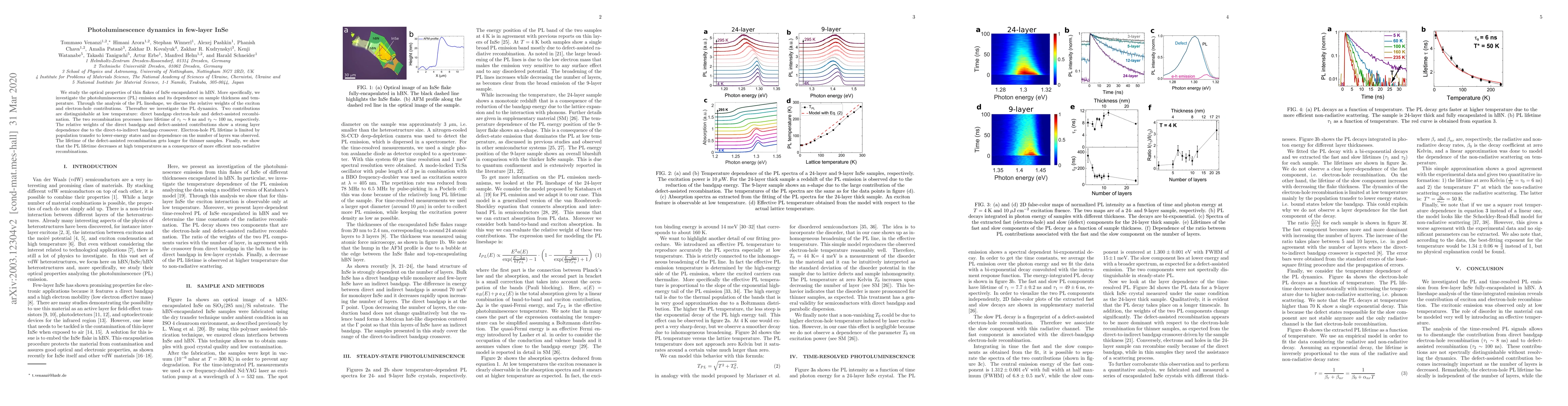
We study the optical properties of thin flakes of InSe encapsulated in hBN. More specifically, we investigate the photoluminescence (PL) emission and its dependence on sample thickness and temperatu...

Thumbnail for Interlayer band-to-band tunneling and negative differential resistance
  in van der Waals BP/InSe field effect transistors
arXiv
Interlayer band-to-band tunneling and negative differential resistance in van der Waals BP/InSe field effect transistors

Atomically thin layers of van der Waals (vdW) crystals offer an ideal material platform to realize tunnel field effect transistors (TFETs) that exploit the tunneling of charge carriers across the fo...

Thumbnail for Design of van der Waals Interfaces for Broad-Spectrum Optoelectronics
arXiv
Design of van der Waals Interfaces for Broad-Spectrum Optoelectronics

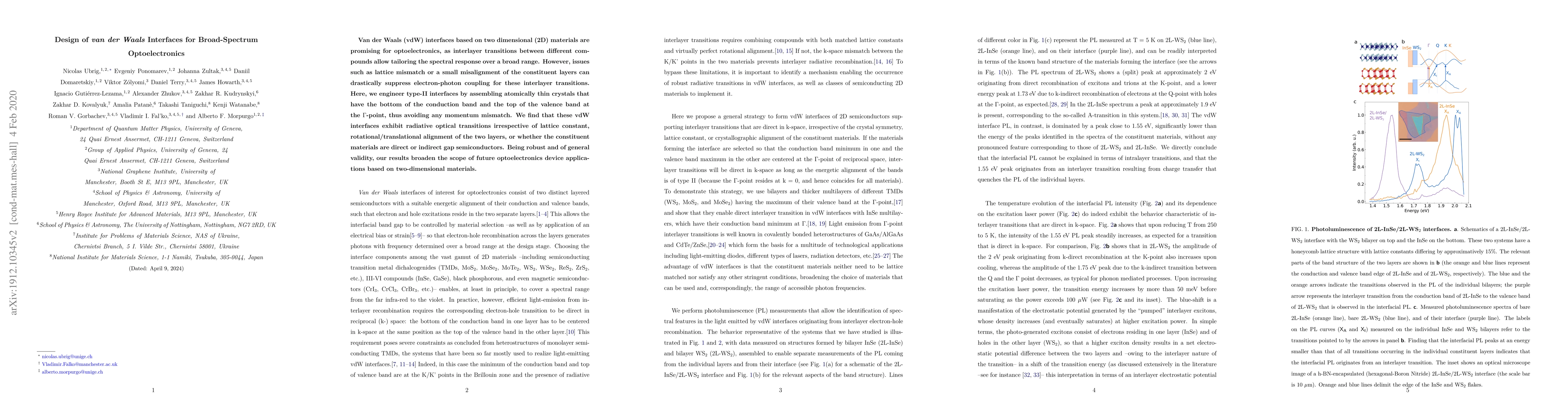
Van der Waals (vdW) materials offer new ways to assemble artificial electronic media with properties controlled at the design stage, by combining atomically defined layers into interfaces and hetero...

Thumbnail for Two-dimensional covalent crystals by chemical conversion of thin van der
  Waals materials
arXiv
Two-dimensional covalent crystals by chemical conversion of thin van der Waals materials

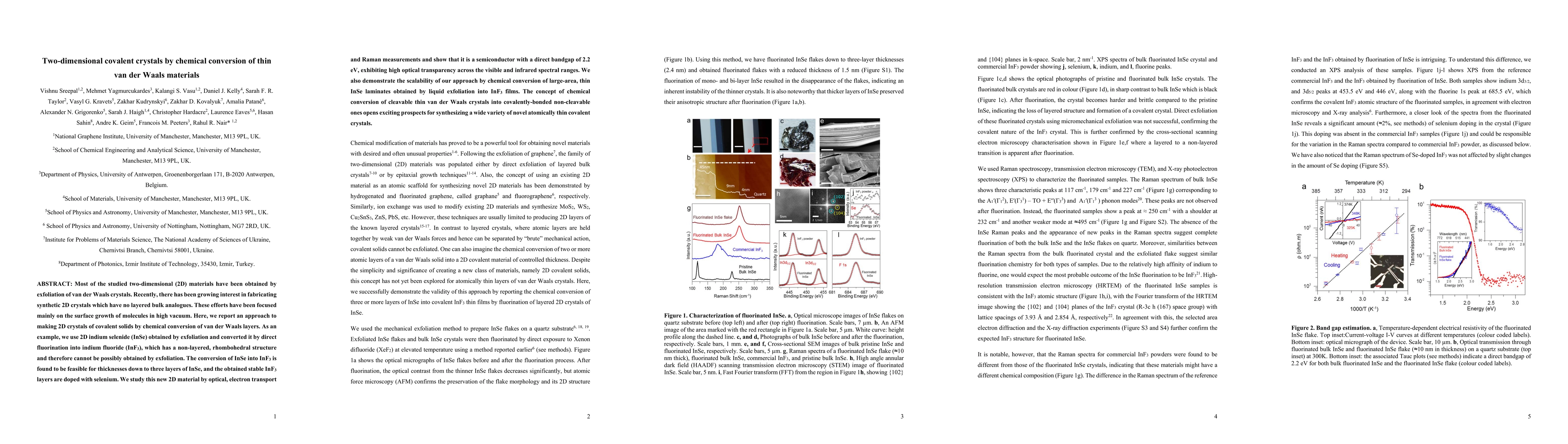
Most of the studied two-dimensional (2D) materials have been obtained by exfoliation of van der Waals crystals. Recently, there has been growing interest in fabricating synthetic 2D crystals which h...

Thumbnail for Two-dimensional magnetic tunnel p-n junctions for low-power electronics
arXiv
Two-dimensional magnetic tunnel p-n junctions for low-power electronics

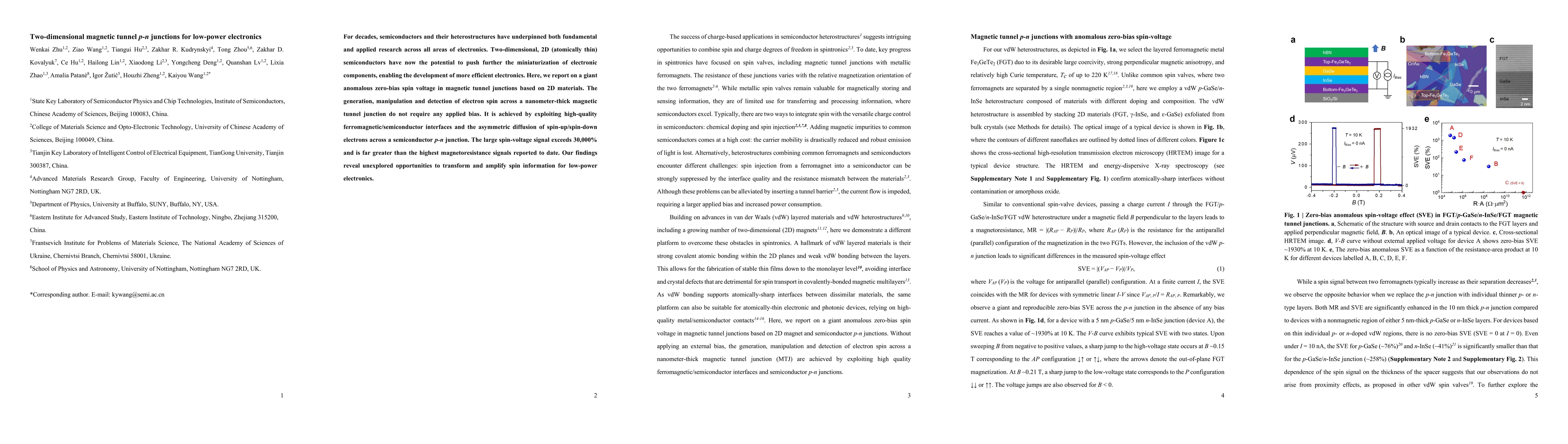
For decades, semiconductors and their heterostructures have underpinned both fundamental and applied research across all areas of electronics. Two-dimensional, 2D (atomically thin) semiconductors have...

This website uses cookies to ensure you get the best experience. Learn more