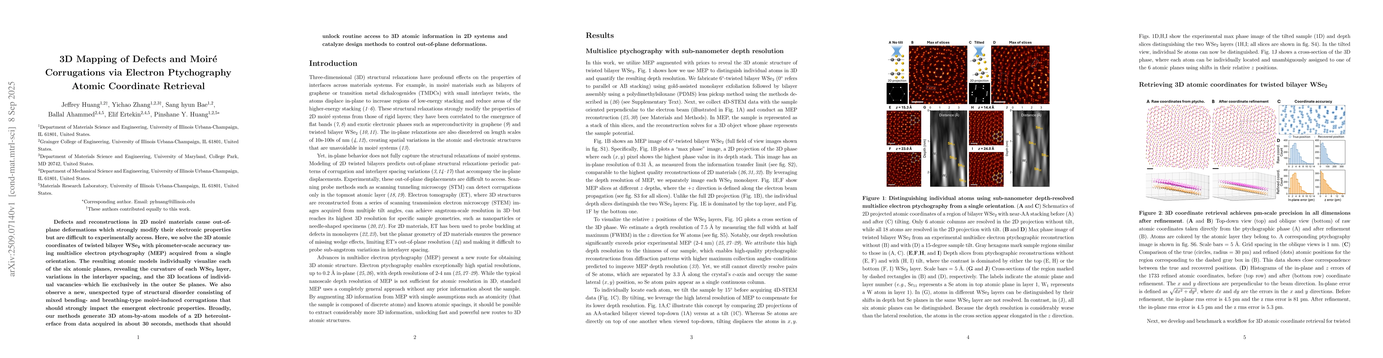
Defects and reconstructions in 2D moir\'e materials cause out-of-plane
deformations which strongly modify their electronic properties but are
difficult to experimentally access. Here, we solve the 3D atomic coordinates of
twisted bilayer WSe$_2$ with picometer-scale accuracy using multislice electron
ptychography (MEP) acquired from a single orientation. The resulting atomic
models individually visualize each of the six atomic planes, revealing the
curvature of each WSe$_2$ layer, variations in the interlayer spacing, and the
3D locations of individual vacancies -- which lie exclusively in the outer Se
planes. We also observe a new, unexpected type of structural disorder
consisting of mixed bending -- and breathing-type moir\'e-induced corrugations
that should strongly impact the emergent electronic properties. Broadly, our
methods generate 3D atom-by-atom models of a 2D heterointerface from data
acquired in about 30 seconds, methods that should unlock routine access to 3D
atomic information in 2D systems and catalyze design methods to control
out-of-plane deformations.
Discussion 0