The paper introduces a new transfer technique that enables high-mobility graphene devices on commercially available hexagonal boron nitride, achieving mobilities up to 275,000 cm²/V/s at 4.2 K, supported by quantum Hall plateau development, and produces bubble- and wrinkle-free graphene on boron nitride substrates.
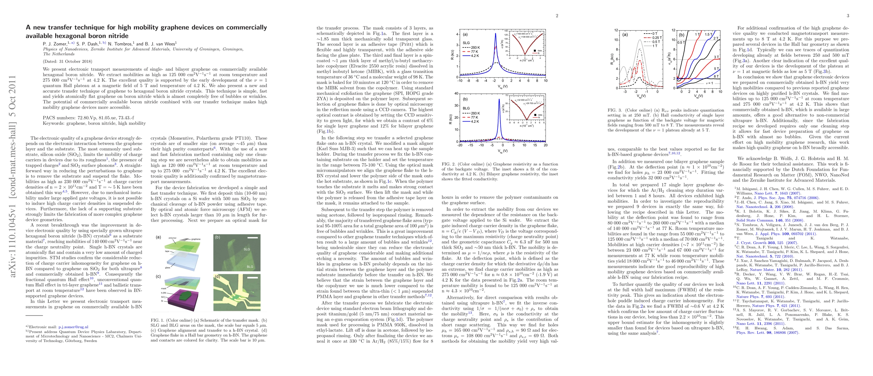
We present electronic transport measurements of single- and bilayer graphene on commercially available hexagonal boron nitride. We extract mobilities as high as 125 000 cm^2/V/s at room temperature and 275 000 cm^2/V/s at 4.2 K. The excellent quality is supported by the early development of the nu = 1 quantum Hall plateau at a magnetic field of 5 T and temperature of 4.2 K. We also present a new and accurate transfer technique of graphene to hexagonal boron nitride crystals. This technique is simple, fast and yields atomically flat graphene on boron nitride which is almost completely free of bubbles or wrinkles. The potential of commercially available boron nitride combined with our transfer technique makes high mobility graphene devices more accessible.
This graph shows how this paper is connected to other research. The current paper is shown in dark gray, papers that cite it are in green, and papers it references are in blue. You can:
• Hover over any node to see the paper title
• Click a node to view that paper's details
• Drag nodes to rearrange the graph
• Use the zoom controls (bottom right) to zoom in/out
Title | Authors | Year | Actions |
---|---|---|---|
A comprehensive Review based on the synthesis, properties, morphology, functionalization, and potential applications of transition metals nitrides
|
Hamid Ali, Yasin Orooji, Z. Ajmal, Mohamed Abboud, A. Abu‐Dief, Khulood A. Abu Al-Ola, Hassan M.A. Hassan, Dewu Yue, Sheng-Rong Guo, Asif Hayat
|
2025
|
View Paper |
Role of graphene in metal matrix functional composites: a review
|
Vignesh Babu Rajendren, Muhammad Raies Abdullah, Farooq Ahmad, Sami Ullah Khan, S. Dar, Xizhou Kai, Yutao Zhao
|
2024
|
View Paper |
Edge Dependence of Nonlocal Transport in Gapped Bilayer Graphene.
|
Hyeon-Woo Jeong, Seong Jang, Sein Park, Kenji Watanabe, T. Taniguchi, Gil-Ho Lee
|
2024
|
View Paper |
Graphene MEMS and NEMS
|
Xuge Fan, Chang He, Jie Ding, Qiang Gao, Hongliang Ma, M. C. Lemme, Wendong Zhang
|
2024
|
View Paper |
Direct visualization of relativistic quantum scars in graphene quantum dots.
|
Zhehao Ge, A. M. Graf, J. Keski-Rahkonen, S. Slizovskiy, Peter Polizogopoulos, T. Taniguchi, Kenji Watanabe, Ryan Van Haren, David Lederman, V. Fal’ko, E. J. Heller, J. Velasco
|
2024
|
View Paper |
Ni(111) Substrate Engineering for the Epitaxial Chemical Vapor Deposition Growth of Wrinkle-Free Multilayer Rhombohedral Boron Nitride Films
|
Laure Tailpied, A. Andrieux-Ledier, F. Fossard, J. Mérot, J. Decams, Annick Loiseau
|
2024
|
View Paper |
Advances in 2D Material Transfer Systems for van der Waals Heterostructure Assembly
|
R. Somphonsane, Kanokwan Buapan, Harihara Ramamoorthy
|
2024
|
View Paper |
Quantitative regulation of electron–phonon coupling
|
Shenghai Pei, Zejuan Zhang, Chenyin Jiao, Zhenyu Wang, Jian Lv, Yujun Zhang, Mingyuan Huang, Yanchao Wang, Zenghui Wang, Juan Xia
|
2024
|
View Paper |
Fabrication of pristine 2D heterostructures for scanning probe microscopy
|
James McKenzie, Nileema Sharma, Xiaolong Liu
|
2024
|
View Paper |
Oblique spin injection to graphene via geometry controlled magnetic nanowires
|
J. Toscano-Figueroa, Daniel Burrow, V. Guarochico-Moreira, Chengkun Xie, Thomas Thomson, Irina V. Grigorieva, I. J. Vera-Marun
|
2024
|
View Paper |
Transfer of 2D Films: From Imperfection to Perfection
|
P. Pham, Theresa Mai, S. Dash, Vasudevanpillai Biju, Y. Chueh, D. Jariwala, Vincent Tung
|
2024
|
View Paper |
Shape memory polymer assisted transfer printing of large-area metal thin film
|
Yawen Gan, Kaiqi Chen, Jingyang Zhang, Qinhua Guo, Yunda Wang
|
2024
|
View Paper |
Layer-by-Layer Self-Assembly Strategies of Atomically Thin Two-Dimensional Nanomaterials: Principles, Methods, and Functional Applications
|
M. Cai, Jianfang Yang, Xueyi Lu, Xia Lu
|
2024
|
View Paper |
Strongly enhanced nonlinear acoustic valley Hall effect in tilted Dirac materials
|
Jia-Liang Wan, Ying-Li Wu, Ke-Qiu Chen, Xiao-Qin Yu
|
2024
|
View Paper |
2D multifunctional devices: from material preparation to device fabrication and neuromorphic applications
|
Zhuohui Huang, Yanran Li, Yi Zhang, Jiewei Chen, Jun He, Jie Jiang
|
2024
|
View Paper |
Terahertz amplification and lasing in pump-probe experiments with hyperbolic polaritons in h-BN
|
Kh. G. Nazaryan, Ivan Ridkokasha, Marios H. Michael, E. Demler
|
2024
|
View Paper |
Quasi-one-dimensional transport in graphene under a magnetic field
|
Minsoo Kim
|
2024
|
View Paper |
Thermal Rectification across an Asymmetric Layer Carbon Nanotube van der Waals Heterostructure.
|
Ning Wu, Yingguang Liu, Shuo Wang, Zhibo Xing
|
2024
|
View Paper |
Progress and prospects in two-dimensional magnetism of van der Waals materials
|
Youngjun Ahn, Xiaoyu Guo, Suhan Son, Zeliang Sun, Liuyan Zhao
|
2024
|
View Paper |
Engineering the flexibility of graphene/h-BN lateral heterojunctions
|
Yi Li, Lizhao Liu, Xiaoming Huang
|
2024
|
View Paper |
Polarization-selective equilibration and quantum interference in graphene-based quantum Hall edge states
|
Minsoo Kim
|
2023
|
View Paper |
Origin of minimal conductivity in Dirac materials: Momentum-dependent self-energy function from long-ranged disorder scattering
|
Weiwei Chen, Yedi Shen, Bo Fu, Qinwei Shi, W. Zhu
|
2023
|
View Paper |
High-efficiency dual single layer graphene modulator integrated on slot waveguides.
|
Chenghan Wu, T. Reep, S. Brems, Julien Jussot, V. Mootheri, J. Van Campenhout, Cedric Huyghebaert, M. Pantouvaki, Zheng Wang, D. van Thourhout
|
2023
|
View Paper |
Origin of electrical noise near charge neutrality in dual gated graphene device
|
Aaryan Mehra, R. Mathew, Chandan Kumar
|
2023
|
View Paper |
Quasiparticle and transport properties of disordered bilayer graphene
|
Yanru Chen, Bo Fu, Jin-Rong Xu, Q. Shi, P. Cui, Zhenyu Zhang
|
2023
|
View Paper |
Disorder effects on the quasiparticle and transport properties of two-dimensional Dirac fermionic systems
|
Bo Fu, Yanru Chen, Weiwei Chen, Wei Zhu, P. Cui, Qunxiang Li, Zhenyu Zhang, Q. Shi
|
2023
|
View Paper |
Catalytic formic acid dehydrogenation via hexagonal-boron nitride supported palladium
|
Zhile Miao, Rongjun Zhang, Hongwei Li, Yu Wu, Zhao Sun, Yan Yu, Zhi-qiang Sun
|
2023
|
View Paper |
Wafer‐Scale Integration of Single Layer Graphene Electro‐Absorption Modulators in a 300 mm CMOS Pilot Line
|
Cheng-Long Wu, S. Brems, D. Yudistira, D. Cott, A. Milenin, K. Vandersmissen, A. Maestre, A. Centeno, A. Zurutuza, J. Van Campenhout, C. Huyghebaert, D. van Thourhout, M. Pantouvaki
|
2023
|
View Paper |
Hydroxyl Boron Nitrid e/Natural Rubber Composites with Enhanced Mechanical and Thermal Conduction Properties: Implications for Heat Dissipative Tires or Conveyor Belts
|
Zhiying Li, Fuhai Guo, Sheng Tian, Ru Liu, Dongchun Yang, X. Wang, Haiqing Hu, Yilong Wang, Jian Zhao
|
2023
|
View Paper |
Fabrication and applications of van der Waals heterostructures
|
Junlei Qi, Zongxiao Wu, Wenbin Wang, Kaijing Bao, Lingzhi Wang, Jingkun Wu, Chengxuan Ke, Yue Xu, Qiyuan He
|
2023
|
View Paper |
Inducing superconductivity in bilayer graphene by alleviation of the Stoner blockade
|
Gal Shavit, Y. Oreg
|
2023
|
View Paper |
Eddy Current Measurement of Chemiresistive Sensing Transients in Graphene-hBN Heterostructures.
|
Manasi Doshi, Jie Zhang, E. Fahrenthold
|
2022
|
View Paper |
Determining spin-orbit coupling in graphene by quasiparticle interference imaging
|
Lihuan Sun, L. Rademaker, Diego Mauro, A. Scarfato, Árpád Pásztor, Ignacio Gutiérrez-Lezama, Zhe Wang, J. Martinez-Castro, A. Morpurgo, C. Renner
|
2022
|
View Paper |
Giant orbital magnetic moments and paramagnetic shift in artificial relativistic atoms and molecules
|
Zhehao Ge, S. Slizovskiy, Peter Polizogopoulos, T. Joshi, T. Taniguchi, Kenji Watanabe, D. Lederman, V. Fal’ko, J. Velasco
|
2022
|
View Paper |
Two-dimensional devices and integration towards the silicon lines
|
Shuiyuan Wang, Xiaoxian Liu, Mingsheng Xu, Liwei Liu, Deren Yang, P. Zhou
|
2022
|
View Paper |
2D Van der Waals Heterostructures for Chemical Sensing
|
Hui‐Lei Hou, Cosimo Anichini, P. Samorí, A. Criado, Maurizio Prato
|
2022
|
View Paper |
Recent progress in 2D van der Waals heterostructures: fabrication, properties, and applications
|
Zenghui Wang, Bo Xu, Shenghai Pei, Jiankai Zhu, Ting Wen, Chenyin Jiao, Jing Li, Mao Zhang, Juan Xia
|
2022
|
View Paper |
Programmable Photo‐Induced Doping in 2D Materials
|
S. Aftab, M. Z. Iqbal, M. W. Iqbal
|
2022
|
View Paper |
Effects of Mono-Vacancies and Co-Vacancies of Nitrogen and Boron on the Energetics and Electronic Properties of Heterobilayer h-BN/graphene
|
G. C. Jiménez, Juan David Morinson-Negrete, Franklin Peniche Blanquicett, C. Ortega-López, Miguel J. Espitia-Rico
|
2022
|
View Paper |
A brief review on the spin valve magnetic tunnel junction composed of 2D materials
|
Ehsan Elahi, Ghulam Dastgeer, P. Sharma, S. Nisar, Muhammad Suleman, M. W. Iqbal, M. Imran, Muhammad Aslam, A. Imran
|
2022
|
View Paper |
Preparation and performance of a composite epoxy coating based on modified hydroxyapatite
|
Y. Guo, Zongxue Yu, Legang Chen, Kexi Liao, Haidong Chen, Yao Pang, Bokai Peng, Lijuan Zhu
|
2022
|
View Paper |
Van der Waals heterostructures
|
A. Castellanos-Gomez, Xiangfeng Duan, Zhe Fei, H. R. Gutierrez, Yuanhao Huang, Xinyu Huang, Jorge Quereda, Qi Qian, E. Sutter, P. Sutter
|
2022
|
View Paper |
Microwave Synthesized 2D Gold and Its 2D-2D Hybrids.
|
Sumita Chahal, Arkamita Bandyopadhyay, S. Dash, Prashant Kumar
|
2022
|
View Paper |
Band Gap Opening in Bilayer Graphene-CrCl3/CrBr3/CrI3 van der Waals Interfaces.
|
Giulia Tenasini, David Soler-Delgado, Zhe Wang, Fengrui Yao, D. Dumcenco, E. Giannini, Kenji Watanabe, T. Taniguchi, C. Moulsdale, A. Garcia-Ruiz, V. Fal’ko, Ignacio Gutiérrez-Lezama, A. Morpurgo
|
2022
|
View Paper |
Tunable biaxial strain device for low-dimensional materials.
|
V. Pasquier, A. Scarfato, J. Martinez-Castro, A. Guipet, C. Renner
|
2022
|
View Paper |
Probing Magnetism in Exfoliated VI3 Layers with Magnetotransport.
|
David Soler-Delgado, Fengxue Yao, D. Dumcenco, E. Giannini, Jiaruo Li, C. Occhialini, R. Comin, N. Ubrig, A. Morpurgo
|
2022
|
View Paper |
High-Performance All-Optical Modulator Based on Graphene-HBN Heterostructures
|
Mohammed Alaloul, J. Khurgin
|
2022
|
View Paper |
Constructing van der Waals heterostructures by dry-transfer assembly for novel optoelectronic device
|
Huihan Li, Xiaolu Xiong, F. Hui, Dongliang Yang, Jinbao Jiang, W. Feng, Junfeng Han, J. Duan, Zhongrui Wang, Linfeng Sun
|
2022
|
View Paper |
Dry Transfer Process of Single-Layer Graphene on Multi-Layer Hexagonal Boron Nitride for High Quality Heterostructure
|
Alireza Kalantari, Yusefi Mostafa, Shaharin Fadzli Abd. Rahman, A. M. Hashim
|
2022
|
View Paper |
Zigzag graphene nanoribbon antidot lattice for local interconnect applications: a precise computational method
|
Mehnoush Arjmandian, H. Karamitaheri, H. K. Alidash
|
2022
|
View Paper |
Challenges and opportunities in 2D heterostructures for electronic and optoelectronic devices
|
S. Chakraborty, Baisali Kundu, B. Nayak, S. Dash, P. Sahoo
|
2022
|
View Paper |
Fano factor in self-similar multibarrier structure based on graphene monolayer
|
M. Miniya, O. Oubram, A. E. El Hachimi, L. Gaggero-Sager
|
2022
|
View Paper |
Light sources with bias tunable spectrum based on van der Waals interface transistors
|
H. Henck, Diego Mauro, D. Domaretskiy, M. Philippi, S. Memaran, Wenkai Zheng, Zhengguang Lu, D. Shcherbakov, C. N. Lau, D. Smirnov, L. Balicas, Kenji Watanabe, T. Taniguchi, V. Fal’ko, Ignacio Gutiérrez-Lezama, N. Ubrig, A. Morpurgo
|
2022
|
View Paper |
Facile fabrication of 2D material multilayers and vdW heterostructures with multimodal microscopy and AFM characterization
|
S. Dong, Xiang Zhang, S. S. P. Nathamgari, A. Krayev, Xu Zhang, Jin Wook Hwang, P. Ajayan, H. Espinosa
|
2022
|
View Paper |
Progress in epitaxial growth of stanene
|
M. Ochapski, M. D. de Jong
|
2022
|
View Paper |
Effect of boron nitride defects and charge inhomogeneity on 1/f noise in encapsulated graphene
|
Chandan Kumar, A. Das
|
2021
|
View Paper |
Emerging van der Waals junctions based on TMDs materials for advanced gas sensors
|
Wei Zheng, Xianghong Liu, Jiayue Xie, Guo-min Lu, Jun Zhang
|
2021
|
View Paper |
Peeling of graphene/molybdenum disulfide heterostructure at different angles: A continuum model with accommodations for van der Waals interaction
|
Zi Wei, Kui Lin, Xiaohe Wang, Ya-pu Zhao
|
2021
|
View Paper |
Van der Waals
Heterostructures in Photocatalytic Energy Conversion
|
Bikesh Gupta, Han Li, J. Tournet, H. Tan, C. Jagadish, Shaowen Cao, S. Karuturi
|
2021
|
View Paper |
Steering on Degrees of Freedom of 2D Van der Waals Heterostructures
|
Huizhen Zhang, Wenjing Wu, Lin Zhou, Zhen Wu, Jia Zhu
|
2021
|
View Paper |
Highly Accurate, Reliable and Non-Contaminating Two-Dimensional Material Transfer System
|
C. Patil, H. Dalir, Jin Ho Kang, Albert V. Davydov, C. W. Wong, V. Sorger
|
2021
|
View Paper |
On the sample-dependent minimal conductivity in weakly disordered graphene
|
Weiwei Chen, Yedi Shen, Bo Fu, Q. Shi, W. Zhu
|
2021
|
View Paper |
When graphene meets white graphene - recent advances in the construction of graphene and h-BN heterostructures.
|
Ziyi Han, Menghan Li, Lin Li, Fei Jiao, Zhongming Wei, Dechao Geng, Wenping Hu
|
2021
|
View Paper |
Material considerations for the design of 2D/3D hot electron transistors
|
Furkan Turker, S. Rajabpour, J. Robinson
|
2021
|
View Paper |
Conversion of electromagnetic wave into propagating plasmon in a periodic graphene structure
|
D. Fateev, I. Moiseenko, K. Mashinsky, V. Popov
|
2021
|
View Paper |
Energy spectrum of bilayer graphene with magnetic quantum structures studied using the Dirac equation
|
D. Park, Heesang Kim, N. Kim
|
2021
|
View Paper |
Heated Assembly and Transfer of Van der Waals Heterostructures with Common Nail Polish
|
Kristine L. Haley, Jeffrey A. Cloninger, Kayla Cerminara, Randy M. Sterbentz, T. Taniguchi, Kenji Watanabe, J. Island
|
2021
|
View Paper |
Electronic states of graphene quantum dots induced by nanobubbles
|
H. Park, Minsol Son, Seung Joo Lee, N. Myoung
|
2021
|
View Paper |
Surface states and quasiparticle interference in Bernal and rhombohedral graphite with and without trigonal warping
|
V. Kaladzhyan, Sarah Pinon, F. Joucken, Zhehao Ge, E. Quezada-López, T. Taniguchi, K. Watanabe, J. Velasco, C. Bena
|
2021
|
View Paper |
Sublattice Dependence and Gate Tunability of Midgap and Resonant States Induced by Native Dopants in Bernal-Stacked Bilayer Graphene.
|
F. Joucken, C. Bena, Zhehao Ge, E. Quezada-López, F. Ducastelle, Takashi Tanagushi, Kenji Watanabe, J. Velasco
|
2021
|
View Paper |
Direct Visualization of Native Defects in Graphite and Their Effect on the Electronic Properties of Bernal-Stacked Bilayer Graphene.
|
F. Joucken, C. Bena, Zhehao Ge, E. Quezada-López, Sarah Pinon, V. Kaladzhyan, T. Taniguchi, Kenji Watanabe, Aires Ferreira, J. Velasco
|
2021
|
View Paper |
Impact of Graphene or Reduced Graphene Oxide on Performance of Thermoelectric Composites
|
O. Okhay, A. Tkach
|
2021
|
View Paper |
Control of Giant Topological Magnetic Moment and Valley Splitting in Trilayer Graphene.
|
Zhehao Ge, S. Slizovskiy, F. Joucken, Eberth A. Quezada, T. Taniguchi, Kenji Watanabe, V. Falko, J. Velasco
|
2021
|
View Paper |
Proximity Effect of Epitaxial Iron Phthalocyanine Molecules on High-Quality Graphene Devices
|
Haiyang Pan, Xiaobo Wang, Qiaoming Wang, Xiaohua Wu, Chang Liu, Nian-Cin Lin, Yuelin Zhao
|
2021
|
View Paper |
Recent mechanical processing techniques of two-dimensional layered materials: A review
|
Xuguang Cao, Chengming Jiang, Dongchen Tan, Qikun Li, Sheng Bi, Jinhui Song
|
2021
|
View Paper |
Damage-Free Atomic Layer Etch of WSe2: A Platform for Fabricating Clean Two-Dimensional Devices.
|
Ankur Nipane, Min Sup Choi, Punnu Jose Sebastian, K. Yao, Abhinandan Borah, P. Deshmukh, Younghun Jung, Bumho Kim, Anjaly Rajendran, K. Kwock, A. Zangiabadi, Vinod M. Menon, P. J. Schuck, Won Jong Yoo, J. Hone, J. Teherani
|
2020
|
View Paper |
Deterministic transfer of optical-quality carbon nanotubes for atomically defined technology
|
K. Otsuka, N. Fang, D. Yamashita, T. Taniguchi, Kenji Watanabe, Y. Kato
|
2020
|
View Paper |
Wafer‐scale
vertical van der
Waals
heterostructures
|
Lixin Liu, T. Zhai
|
2020
|
View Paper |
Optoelectronic Properties of Nanocarbons and Nanocarbon Films
|
C. Shearer, Le-Yong Yu, J. Shapter
|
2020
|
View Paper |
Polymer-assisted TEM specimen preparation method for oxidation-sensitive 2D materials
|
J. Köster, Baokun Liang, A. Storm, U. Kaiser
|
2020
|
View Paper |
Stacking of 2D Materials
|
Hao-Wei Guo, Zhen Hu, Zhi-bo Liu, J. Tian
|
2020
|
View Paper |
Dielectric Transfer Process for 3D Printed Metal Microsystems
|
Bhushan Lohani, Sheikh Dobir Hossain, R. Roberts
|
2020
|
View Paper |
Electron transport and the effect of current annealing in a two-point contacted hBN/graphene/hBN heterostructure device
|
Leo Schnitzspan, Alexander Tries, M. Kläui
|
2020
|
View Paper |
All-dry Transferred ReS2 Nanosheets for Ultra-sensitive Room-temperature NO2 Sensing under Visible Light Illumination.
|
Junwei Zeng, Yue Niu, Yelei Gong, Quan Wang, Hao Li, A. Umar, N. D. de Rooij, Guofu Zhou, Yao Wang
|
2020
|
View Paper |
Observation of inter-layer charge transmission resonance at optically excited graphene–TMDC interfaces
|
R. Kashid, J. K. Mishra, A. Pradhan, Tanweer Ahmed, S. Kakkar, Pranav S. Mundada, Preeti Deshpande, Kallol Roy, Ambarish Ghosh, Arindam Ghosh
|
2020
|
View Paper |
Group IV elements in 2D structures
|
M. Ochapski
|
2020
|
View Paper |
Two-dimensional electronic devices modulated by the activation of donor-like states in boron nitride.
|
S. Aftab, Samiya, M. W. Iqbal, P. Shinde, A. Rehman, S. Yousuf, Sewon Park, S. Jun
|
2020
|
View Paper |
WSe2 Homojunction p-n Diode Formed by Photo-induced Activation of Mid-gap Defect States in Boron Nitride.
|
S. Aftab, Imtisal Akhtar, Y. Seo, J. Eom
|
2020
|
View Paper |
Enhancement of the thermoelectric properties in bilayer graphene structures induced by Fano resonances
|
J. A. Briones-Torres, R. Pérez-Álvarez, S. Molina-Valdovinos, I. Rodríguez-Vargas
|
2020
|
View Paper |
Towards Scalable Fabrications and Applications of 2D Layered Material-based Vertical and Lateral Heterostructures
|
Xi Wan, Hao Li, Kun Chen, Jianbin Xu
|
2020
|
View Paper |
Comprehensive Electrostatic Modeling of Exposed Quantum Dots in Graphene/Hexagonal Boron Nitride Heterostructures
|
E. Quezada-López, Zhehao Ge, T. Taniguchi, Kenji Watanabe, F. Joucken, J. Velasco
|
2020
|
View Paper |
Van der waals heterojunctions for catalysis
|
Yibo Yan, Zhiping Zeng, Ming Huang, Peng Chen
|
2020
|
View Paper |
Integrated single photon emitters
|
Junyi Lee, V. Leong, D. Kalashnikov, Jibo Dai, Alagappan Gandhi, L. Krivitsky
|
2020
|
View Paper |
Thermal annealing effect on the electrical quality of graphene/hexagonal boron nitride heterostructure devices
|
Haiyang Pan, Qiaoming Wang, Xiaohua Wu, Tingting Song, Q. Song, Jue Wang
|
2020
|
View Paper |
Spin caloritronics in a
CrBr3-based
magnetic van der Waals heterostructure
|
Tian Liu, J. Peiro, Dennis K. de Wal, J. Leutenantsmeyer, M. Guimarães, B. V. van Wees
|
2020
|
View Paper |
Low-dimensional thermoelectricity in aperiodic gated graphene superlattices
|
S. Molina-Valdovinos, E. J. Guzmán, I. Rodríguez-Vargas
|
2020
|
View Paper |
Giant ac magnetoconductivity in rGO-Fe3O4 composites
|
Khush Bakhat Akram, S. Z. U. Hassan, Awais Ahmed, Muhammad Hamayun, M. Rafique, S. Manzoor
|
2020
|
View Paper |
Evidence for Electron Transfer between Graphene and Non‐Covalently Bound π‐Systems
|
Steffen M. Brülls, Valentina Cantatore, Zhenping Wang, P. Tam, P. Malmberg, J. Stubbe, B. Sarkar, I. Panas, J. Mårtensson, Siegfried Eigler
|
2020
|
View Paper |
Facile deterministic cutting of 2D materials for twistronics using a tapered fibre scalpel
|
L. D. V. Sangani, Surya Kanthi R S, Pratap Chandra Adak, Subhajit Sinha, Alisha H. Marchawala, T. Taniguchi, Kenji Watanabe, M. Deshmukh
|
2020
|
View Paper |
Two-dimensional tunable polarization-dependent absorptions for binary and ternary coding
|
Huan Jiang, Ying Cui, Yongyuan Jiang
|
2020
|
View Paper |
Propagating plasmon in periodical graphene structure
|
K. V. Mashinskiy, V. Popov, M. Morozov, D. Fateev
|
2020
|
View Paper |
Transfer assembly for two-dimensional van der Waals heterostructures
|
Sidi Fan, Q. Vu, Minh Dao Tran, S. Adhikari, Y. H. Lee
|
2020
|
View Paper |
A system for the deterministic transfer of 2D materials under inert environmental conditions
|
Patricia Gant, F. Carrascoso, Qinghua Zhao, Y. Ryu, Michael Seitz, F. Prins, R. Frisenda, A. Castellanos-Gomez
|
2020
|
View Paper |
Manufacturing strategies for wafer-scale two-dimensional transition metal dichalcogenide heterolayers
|
Mengjing Wang, Hao Li, T. Ko, Mashiyat Sumaiya Shawkat, E. Okogbue, Changhyeon Yoo, S. Han, Md. Ashraful Islam, K. Oh, Yeonwoong Jung
|
2020
|
View Paper |
Influence of Coupling Strength Between a Magnetic Quantum Dot and Quantum Hall Edge Channels on Valley-isospin-dependent Dirac Fermion Transport
|
Jihyeon Jeon, Minsol Son, N. Myoung
|
2020
|
View Paper |
An inexpensive system for the deterministic transfer of 2D materials
|
Qinghua Zhao, Tao Wang, Y. Ryu, R. Frisenda, A. Castellanos-Gomez
|
2020
|
View Paper |
Persistent and reversible electrostatic control of doping in graphene/hexagonal boron nitride heterostructures
|
E. Quezada-López, F. Joucken, H. Chen, A. Lara, J. Davenport, K. Hellier, T. Taniguchi, K. Watanabe, S. Carter, A. P. Ramirez, J. Velasco
|
2020
|
View Paper |
Realizing high thermoelectric performance with comparable p- and n-type figure-of-merits in a graphene/h-BN superlattice monolayer.
|
Zizhen Zhou, D. Fan, Huijun Liu
|
2019
|
View Paper |
Determination of the trigonal warping orientation in Bernal-stacked bilayer graphene via scanning tunneling microscopy
|
F. Joucken, Zhehao Ge, Eberth A. Quezada-L'opez, J. Davenport, Kenji Watanabe, T. Taniguchi, J. Velasco
|
2019
|
View Paper |
First Principles Study of the Ambipolarity in a Germanene Nanoribbon Tunneling Field Effect Transistor
|
Azam Samipour, D. Dideban, H. Heidari
|
2019
|
View Paper |
Controlled assembly of artificial 2D materials based on the transfer of oxo-functionalized graphene
|
Marleen Hußmann, Benjamin I. Weintrub, Patrick Feicht, Gregor Germer, J. N. Kirchhof, K. Bolotin, Siegfried Eigler
|
2019
|
View Paper |
Wetting of nanopores probed with pressure.
|
S. Marion, Michał Macha, Sebastian J Davis, A. Chernev, A. Radenović
|
2019
|
View Paper |
Nanobubbles at nanopores probed with pressure
|
S. Marion, Michał Macha, Sebastian J Davis, A. Chernev, A. Radenović
|
2019
|
View Paper |
Mobility Enhancement in Graphene by in situ Reduction of Random Strain Fluctuations.
|
Lujun Wang, P. Makk, S. Zihlmann, A. Baumgartner, David I. Indolese, Kenji Watanabe, T. Taniguchi, C. Schönenberger
|
2019
|
View Paper |
Movable-Type Transfer and Stacking of van der Waals Heterostructures for Spintronics
|
Yuan Cao, Xinhe Wang, Xiaoyang Lin, Wei Yang, Chen Lv, Yuan Lu, Youguang Zhang, Weisheng Zhao
|
2019
|
View Paper |
Electronic structure and scanning tunneling microscopy images of heterostructures consisting of graphene and carbon-doped hexagonal boron nitride layers
|
Taishi Haga, Y. Fujimoto, S. Saito
|
2019
|
View Paper |
Lateral Bilayer MoS2–WS2 Heterostructure Photodetectors with High Responsivity and Detectivity
|
Kun Ye, Lixuan Liu, Yujie Liu, A. Nie, K. Zhai, J. Xiang, Bochong Wang, F. Wen, C. Mu, Zhisheng Zhao, Y. Gong, Zhongyuan Liu, Yongjun Tian
|
2019
|
View Paper |
Axial field induced spin response in Fe/hBN-based tunnel junctions
|
A. M. Ukpong
|
2019
|
View Paper |
Adsorption and epitaxial growth of small organic semiconductors on hexagonal boron nitride
|
M. Kratzer, A. Matković, C. Teichert
|
2019
|
View Paper |
Graphene Hybrid Structures for Integrated and Flexible Optoelectronics
|
Xiaoqing Chen, Khurram Shehzad, Li Gao, M. Long, Hui Guo, Shuchao Qin, Xiaomu Wang, Fengqiu Wang, Yi Shi, Weida Hu, Yang Xu, Xinran Wang
|
2019
|
View Paper |
Growth of Multi-Layer hBN on Ni(111) Substrates via MOCVD
|
G. Siegel, Gordon Gryzbowcki, A. Hilton, C. Muratore, M. Snure
|
2019
|
View Paper |
Enhancing sensitivity to ambient refractive index with tunable few-layer graphene/hBN nanoribbons
|
Huan Jiang, S. Choudhury, Z. Kudyshev, Di Wang, L. Prokopeva, Peng Xiao, Yongyuan Jiang, A. Kildishev
|
2019
|
View Paper |
Fractional and Symmetry-Broken Chern Insulators in Tunable Moiré Superlattices.
|
B. Cheng, C. Pan, Shi Che, Peng Wang, Yong Wu, Kenji Watanabe, T. Taniguchi, Supeng Ge, R. Lake, D. Smirnov, C. N. Lau, M. Bockrath
|
2019
|
View Paper |
Excitation of Propagating Plasmons in a Periodic Graphene Structure by Incident Terahertz Waves
|
D. Fateev, K. Mashinsky, O. Polischuk, V. Popov
|
2019
|
View Paper |
Design of an Electro-Absorption Modulator Based on Graphene-on-Silicon Slot Waveguide
|
Lanting Ji, Da-ming Zhang, Yan Xu, Yang Gao, Chi Wu, Xi-bin Wang, Zhiyong Li, Xiaoqiang Sun
|
2019
|
View Paper |
Mechanical and liquid phase exfoliation of cylindrite: a natural van der Waals superlattice with intrinsic magnetic interactions
|
Yue Niu, J. Villalva, R. Frisenda, G. Sánchez-Santolino, L. Ruiz-González, E. Pérez, M. Garc'ia-Hern'andez, E. Burzur'i, A. Castellanos-Gomez
|
2019
|
View Paper |
Thickness determination of MoS2, MoSe2, WS2 and WSe2 on transparent stamps used for deterministic transfer of 2D materials
|
N. S. Taghavi, Patricia Gant, Peng Huang, I. Niehues, R. Schmidt, S. Michaelis de Vasconcellos, R. Bratschitsch, M. García-Hernández, R. Frisenda, A. Castellanos-Gomez
|
2019
|
View Paper |
Cavity Enhanced Trion Emission from a Bilayer MoTe 2 on Silicon
|
Jianxing Zhang, Zizhao Zhong, Yongzhuo Li, Jiabin Feng, Lin Gan, C. Ning
|
2019
|
View Paper |
Nanospot angle-resolved photoemission study of Bernal-stacked bilayer graphene on hexagonal boron nitride: Band structure and local variation of lattice alignment
|
F. Joucken, Eberth A. Quezada-L'opez, J. Avila, Chaoyu Chen, J. Davenport, Hechin Chen, Kenji Watanabe, T. Taniguchi, M. Asensio, J. Velasco
|
2019
|
View Paper |
MOCVD Integration Technology of Enestor through Grafene-Like III-Nitride, Nanocarbides and InGaN/GaN QDs
|
V. Osinsky, Nina Sukhoviy, I. Masol, N. Lyahova
|
2019
|
View Paper |
Effects of intercalated atoms on electronic structure of graphene nanoribbon/hexagonal boron nitride stacked layer
|
Dongchul Sung, Gunn Kim, Suklyun Hong
|
2019
|
View Paper |
Flexible Molybdenum Disulfide (MoS2) Atomic Layers for Wearable Electronics and Optoelectronics.
|
Eric Singh, Pragya Singh, Ki Seok Kim, G. Yeom, H. Nalwa
|
2019
|
View Paper |
Ultrahigh Electrical Conductivity of Graphene Embedded in Metals
|
Mu Cao, D. Xiong, Li Yang, Shuaishuai Li, Yiqun Xie, Q. Guo, Zhiqiang Li, H. Adams, Jiajun Gu, T. Fan, Xiaohui Zhang, Di Zhang
|
2019
|
View Paper |
Recent Progress in the Fabrication, Properties, and Devices of Heterostructures Based on 2D Materials
|
Yanping Liu, Siyu Zhang, Jun He, Zhiming M. Wang, Zongwen Liu
|
2019
|
View Paper |
Nonvolatile Memories Based on Graphene and Related 2D Materials
|
Simone Bertolazzi, P. Bondavalli, S. Roche, T. San, Sung‐Yool Choi, L. Colombo, F. Bonaccorso, P. Samorí
|
2019
|
View Paper |
Recent progress in synthesis, properties, and applications of hexagonal boron nitride-based heterostructures
|
J. Meng, Denggui Wang, Likun Cheng, M. Gao, Xingwang Zhang
|
2018
|
View Paper |
Heterostructures of graphene and hBN: Electronic, spin-orbit, and spin relaxation properties from first principles
|
K. Zollner, M. Gmitra, J. Fabian
|
2018
|
View Paper |
Recent advances in the preparation, characterization, and applications of two-dimensional heterostructures for energy storage and conversion
|
Pratteek Das, Q. Fu, X. Bao, Zhong‐Shuai Wu
|
2018
|
View Paper |
Splitting of conductance resonance through a magnetic quantum dot in graphene
|
N. Myoung, J. Ryu, H. Park, Seung Joo Lee, S. Woo
|
2018
|
View Paper |
Direct CVD Growth of Graphene on Technologically Important Dielectric and Semiconducting Substrates
|
Afzal Khan, Sk. Masiul Islam, Shahzad Ahmed, R. Kumar, M. Habib, Kun-Fang Huang, Ming Hu, Xuegong Yu, Deren Yang
|
2018
|
View Paper |
Multilayer graphene shows intrinsic resistance peaks in the carrier density dependence
|
T. Hirahara, R. Ebisuoka, Takushi Oka, Tomoaki Nakasuga, S. Tajima, Kenji Watanabe, T. Taniguchi, R. Yagi
|
2018
|
View Paper |
Recent Advances in Synthesis and Assembly of van der Waals Materials
|
Dongil Chu, E. Kim
|
2018
|
View Paper |
Low-energy band structure and even-odd layer number effect in AB-stacked multilayer graphene
|
R. Yagi, T. Hirahara, R. Ebisuoka, Tomoaki Nakasuga, S. Tajima, Kenji Watanabe, T. Taniguchi
|
2018
|
View Paper |
Electrically Inert h-BN/Bilayer Graphene Interface in All-Two-Dimensional Heterostructure Field Effect Transistors.
|
T. Uwanno, T. Taniguchi, Kenji Watanabe, K. Nagashio
|
2018
|
View Paper |
Visualization and Control of Single-Electron Charging in Bilayer Graphene Quantum Dots.
|
J. Velasco, Juwon Lee, Dillon Wong, S. Kahn, H. Tsai, Joseph Costello, T. Umeda, T. Taniguchi, Kenji Watanabe, A. Zettl, Feng Wang, M. Crommie
|
2018
|
View Paper |
Semiconducting van der Waals Interfaces as Artificial Semiconductors.
|
E. Ponomarev, N. Ubrig, Ignacio Gutiérrez-Lezama, H. Berger, A. Morpurgo
|
2018
|
View Paper |
Low-dimensional thermoelectricity in graphene: The case of gated graphene superlattices
|
S. Molina-Valdovinos, J. Martínez-Rivera, N. E. Moreno-Cabrera, I. Rodríguez-Vargas
|
2018
|
View Paper |
Recent progress in Van der Waals (vdW) heterojunction-based electronic and optoelectronic devices
|
Jaewoo Shim, D. Kang, Yunjo Kim, H. Kum, W. Kong, Sang-Hoon Bae, I. Almansouri, Kyusang Lee, Jin-Hong Park, Jeehwan Kim
|
2018
|
View Paper |
Polarization-independent enhancement of graphene plasmons by coupling with the dipole-like near field of the metallic split-mesh structure
|
A. Yu
|
2018
|
View Paper |
Wafer scale BN on sapphire substrates for improved graphene transport
|
S. Vangala, G. Siegel, T. Prusnick, M. Snure
|
2018
|
View Paper |
Tuning the analog and digital performance of Germanene nanoribbon field effect transistors with engineering the width and geometry of source, channel and drain region in the ballistic regime
|
Hossein Fatholah nejad, D. Dideban, A. Ketabi, Mehran Vali, A. Bayani, H. Heidari
|
2018
|
View Paper |
Coherent transport in Y-junction graphene waveguide
|
Vahid Mosallanejad, K. Chiu, Guoping Guo
|
2018
|
View Paper |
Atomically thin p-n junctions based on two-dimensional materials.
|
R. Frisenda, A. Molina‐Mendoza, T. Mueller, A. Castellanos-Gomez, H. S. van der Zant
|
2018
|
View Paper |
Deterministic and Etching‐Free Transfer of Large‐Scale 2D Layered Materials for Constructing Interlayer Coupled van der Waals Heterostructures
|
Li Tao, Hao Li, Yune Gao, Zefeng Chen, Lei Wang, Ya Deng, Jian Zhang, Jianbin Xu
|
2018
|
View Paper |
Autonomous robotic searching and assembly of two-dimensional crystals to build van der Waals superlattices
|
S. Masubuchi, Masataka Morimoto, Sei Morikawa, Momoko Onodera, Yuta Asakawa, Kenji Watanabe, T. Taniguchi, T. Machida
|
2018
|
View Paper |
Out-of-plane interface dipoles and anti-hysteresis in graphene-strontium titanate hybrid transistor
|
Anindita Sahoo, D. Nafday, Tathagata Paul, R. Ruiter, Arunesh Roy, M. Mostovoy, T. Banerjee, T. Saha‐Dasgupta, A. Ghosh
|
2018
|
View Paper |
Electron scattering in graphene by defects in underlying h-BN layer: First-principles transport calculations
|
T. Kaneko, T. Ohno
|
2018
|
View Paper |
Magnetic field mediated conductance oscillation in graphene p–n junctions
|
Shu-guang Cheng
|
2018
|
View Paper |
Substrate-Dependent Band Structures in Trilayer Graphene/h-BN Heterostructures.
|
Shi Che, P. Stepanov, Supeng Ge, Menglin Zhu, Dongying Wang, Yongjin Lee, K. Myhro, Yanmeng Shi, Ruoyu Chen, Ziqi Pi, C. Pan, B. Cheng, T. Taniguchi, Kenji Watanabe, Y. Barlas, R. Lake, M. Bockrath, Jinwoo Hwang, C. N. Lau
|
2018
|
View Paper |
Twist Angle-Dependent Bands and Valley Inversion in 2D Materials/hBN Heterostructures
|
Shi Che, P. Stepanov, Supeng Ge, Yongjin Lee, K. Myhro, Yanmeng Shi, Ruoyu Chen, Ziqi Pi, C. Pan, B. Cheng, T. Taniguchi, Kenji Watanabe, M. Bockrath, Y. Barlas, R. Lake, C. N. Lau
|
2018
|
View Paper |
2D Photovoltaic Devices: Progress and Prospects
|
Lin Wang, Li Huang, W. Tan, Xuewei Feng, Li Chen, Xin Huang, K. Ang
|
2018
|
View Paper |
Tunable magnetotransport in Fe/hBN/graphene/hBN/Pt(Fe) epitaxial multilayers
|
A. M. Ukpong
|
2018
|
View Paper |
Novel Optoelectronic Devices: Transition‐Metal‐Dichalcogenide‐Based 2D Heterostructures
|
Qingsheng Zeng, Zheng Liu
|
2018
|
View Paper |
2D material printer: a deterministic cross contamination-free transfer method for atomically layered materials
|
R. Hemnani, Jason P. Tischler, Caitlin Carfano, R. Maiti, Mohammad H. Tahersima, L. Bartels, R. Agarwal, V. Sorger
|
2018
|
View Paper |
Electrical spin injection, transport, and detection in graphene-hexagonal boron nitride van der Waals heterostructures: progress and perspectives
|
M. Gurram, S. Omar, B. Wees
|
2017
|
View Paper |
Spin transport in two-layer-CVD-hBN/graphene/hBN heterostructures
|
M. Gurram, S. Omar, S. Zihlmann, P. Makk, Qiucheng Li, Yanfeng Zhang, C. Schonenberger, Bart J. van Wees Physics of Nanodevices, Zernike Institute for Advanced Materials, U. Groningen, Groningen, The Netherlands., D. Physics, U. Basel, Basel, Switzerland., Center for Nanochemistry, Department of Materials Science, Engineering, College of Engineering, P. University, Beijing, P. China
|
2017
|
View Paper |
Equilibration of quantum hall edge states and its conductance fluctuations in graphene p-n junctions
|
Chandan Kumar, Manabendra Kuiri, A. Das
|
2017
|
View Paper |
Recent progress in the assembly of nanodevices and van der Waals heterostructures by deterministic placement of 2D materials.
|
R. Frisenda, E. Navarro-Moratalla, Patricia Gant, D. Perez de Lara, P. Jarillo-Herrero, R. Gorbachev, A. Castellanos-Gomez
|
2017
|
View Paper |
Localization physics in graphene moiré superlattices
|
Chandan Kumar, Saurabh Kumar Srivastav, Priyo Adhikary, S. Banerjee, T. Das, A. Das
|
2017
|
View Paper |
Adsorbate-induced stiffening, quantum thermopower and photoresponse in two-dimensional materials
|
S. Svatek
|
2017
|
View Paper |
Seebeck Coefficient of a Single van der Waals Junction in Twisted Bilayer Graphene.
|
Phanibhusan S. Mahapatra, K. Sarkar, H. R. Krishnamurthy, S. Mukerjee, A. Ghosh
|
2017
|
View Paper |
Proximity coupling in superconductor-graphene heterostructures
|
Gil-Ho Lee, Hu-Jong Lee
|
2017
|
View Paper |
Dry-transferred CVD graphene for inverted spin valve devices
|
M. Drogeler, L. Banszerus, F. Volmer, T. Taniguchi, Kenji Watanabe, B. Beschoten, C. Stampfer
|
2017
|
View Paper |
Electron transport in graphene/h-BN lateral hybrids: Rhombus and bowtie domains
|
A. Mehri, Maryam Jamaati, A. Namiranian
|
2017
|
View Paper |
Improvement in interfacial characteristics of low-voltage carbon nanotube thin-film transistors with solution-processed boron nitride thin films
|
Jun-Young Jeon, T. Ha
|
2017
|
View Paper |
A facile and efficient dry transfer technique for two-dimensional Van derWaals heterostructure*
|
Li Xie, Luojun Du, Xiaobo Lu, Rong Yang, D. Shi, Guangyu Zhang
|
2017
|
View Paper |
Synthesis, structure and applications of graphene-based 2D heterostructures.
|
P. Solís-Fernández, M. Bissett, H. Ago
|
2017
|
View Paper |
Spontaneous doping on high quality talc-graphene-hBN van der Waals heterostructures
|
E. Mania, A. B. Alencar, A. Cadore, B. R. Carvalho, K. Watanabe, T. Taniguchi, B. Neves, H. Chacham, L. C. Campos
|
2017
|
View Paper |
Novel compact antenna designs for future wireless communication systems
|
Christian Núñez-Álvarez
|
2017
|
View Paper |
Optical, photonic and optoelectronic properties of graphene, h-BN and their hybrid materials
|
Jingang Wang, Fengcai Ma, W. Liang, Rongming Wang, Mengtao Sun
|
2017
|
View Paper |
Long-Lived Domain Wall Plasmons in Gapped Bilayer Graphene.
|
E. H. Hasdeo, Justin C. W. Song
|
2017
|
View Paper |
Electrolyte‐induced modulation of electronic transport in the presence of surface charge impurities on bilayer graphene
|
Khush Bakhat Akram, Muhammad Umair Hassan, A. Karim, M. Mehmood, M. Rafiq, Sana Sabahat, S. Manzoor
|
2017
|
View Paper |
Photoresponse of Natural van der Waals Heterostructures.
|
K. Ray, A. E. Yore, Tong Mou, Sauraj Jha, K. Smithe, Bin Wang, E. Pop, A. Newaz
|
2017
|
View Paper |
Molecular Arrangement and Charge Transfer in C60/Graphene Heterostructures.
|
C. Ojeda-Aristizabal, E. Santos, S. Onishi, A. Yan, H. Rasool, S. Kahn, Yinchuan Lv, Drew W. Latzke, J. Velasco, M. Crommie, Matthew Sorensen, Kenneth Gotlieb, Chiu-Yun Lin, Kenji Watanabe, T. Taniguchi, A. Lanzara, A. Zettl
|
2017
|
View Paper |
Layer Polarizability and Easy-Axis Quantum Hall Ferromagnetism in Bilayer Graphene.
|
Cheng Pan, Yong Wu, B. Cheng, Shi Che, T. Taniguchi, Kenji Watanabe, Chun Ning Lau, M. Bockrath
|
2017
|
View Paper |
Quantum optics of electrons in graphene
|
P. Clark
|
2017
|
View Paper |
Recent Development of Boron Nitride towards Electronic Applications
|
N. Izyumskaya, D. Demchenko, Saikat Das, Ü. Özgür, V. Avrutin, H. Morkoç
|
2017
|
View Paper |
Interfacial Engineering of Van der Waals Coupled 2D Layered Materials
|
Hao Hong, Can Liu, Ting Cao, Chenhao Jin, Shaoxin Wang, Feng Wang, Kaihui Liu
|
2017
|
View Paper |
Probing AC electronic compressibility of 3D HgTe and Bi2Se3topological insulators at high electric fields : evidence for excitedmassive surface states
|
A. Inhofer
|
2017
|
View Paper |
The Prospect of Two-Dimensional Heterostructures: A Review of Recent Breakthroughs
|
Daniel S. Schulman, Andrew J Arnold, A. Razavieh, J. Nasr, Saptarshi Das
|
2017
|
View Paper |
Graphene-based Antennas for Terahertz Systems: A Review
|
D. Correas-Serrano, J. S. Gómez-Díaz
|
2017
|
View Paper |
Polarity control of h-BN nanoribbon edges by strain and edge termination.
|
Ayaka Yamanaka, S. Okada
|
2017
|
View Paper |
Electric field effect of GaAs monolayer from first principles
|
Jiongyao Wu, Yali Yang, Heng Gao, Yuting Qi, Jiaqi Zhang, Z. Qiao, W. Ren
|
2017
|
View Paper |
Controlled dynamic screening of excitonic complexes in 2D semiconductors
|
A. Klots, Benjamin I. Weintrub, Dhiraj Prasai, Daniel Kidd, K. Varga, K. Velizhanin, K. Bolotin
|
2017
|
View Paper |
Graphene, hexagonal boron nitride, and their heterostructures: properties and applications
|
Jingang Wang, Fengcai Ma, Mengtao Sun
|
2017
|
View Paper |
A hybrid MBE-based growth method for large-area synthesis of stacked hexagonal boron nitride/graphene heterostructures
|
J. M. Wofford, S. Nakhaie, T. Krause, Xianjie Liu, M. Ramsteiner, M. Hanke, H. Riechert, J. M. J. Lopes
|
2017
|
View Paper |
Quantum dot behavior in transition metal dichalcogenides nanostructures
|
Gang Luo, Zhuo-Zhi Zhang, Haiou Li, Xiang-Xiang Song, Guang-Wei Deng, Gang Cao, M. Xiao, G. Guo
|
2017
|
View Paper |
Transfer of monolayer TMD WS2 and Raman study of substrate effects
|
J. Mlack, Paul Masih Das, Gopinath Danda, Yung-Chien Chou, Carl H. Naylor, Zhong Lin, N. Lopez, Tianyi Zhang, M. Terrones, A. T. Johnson, M. Drndić
|
2017
|
View Paper |
Dirac fermion reflector by ballistic graphene sawtooth-shaped npn junctions
|
Sei Morikawa, Q. Wilmart, S. Masubuchi, Kenji Watanabe, T. Taniguchi, B. Plaçais, T. Machida
|
2017
|
View Paper |
Quantum dot behavior in transition metal dichalcogenides nanostructures
|
Gang Luo, Zhuo-Zhi Zhang, Haiou Li, Xiang-Xiang Song, Guang-Wei Deng, G. Cao, M. Xiao, G. Guo
|
2016
|
View Paper |
Epitaxy of highly ordered organic semiconductor crystallite networks supported by hexagonal boron nitride
|
A. Matković, J. Genser, D. Lüftner, M. Kratzer, R. Gajić, P. Puschnig, C. Teichert
|
2016
|
View Paper |
Méthodologie de fabrication de transistors à base de Graphène : application aux composants optoélectroniques hyperfréquences
|
Sana Mzali
|
2016
|
View Paper |
Theoretical study of electronic and thermoelectric nanodevicesbased on strained graphene junctions
|
M. Nguyen
|
2016
|
View Paper |
Current crowding mediated large contact noise in graphene field-effect transistors
|
P. Karnatak, T. Sai, S. Goswami, S. Ghatak, S. Kaushal, A. Ghosh
|
2016
|
View Paper |
Recent progress of photodetectors based on MX2/graphene van der Waals heterostructures
|
Hang Yang, S. Qin, Jingyue Fang, Gang Peng, Xueao Zhang
|
2016
|
View Paper |
Bandgap engineered graphene and hexagonal boron nitride for resonant tunnelling diode
|
P. Palla, Gopi Raja Uppu, A. Ethiraj, J. Raina
|
2016
|
View Paper |
Room temperature spin valve effect in the NiFe/Gr–hBN/Co magnetic tunnel junction
|
M. Z. Iqbal, S. Siddique, G. Hussain, M. W. Iqbal
|
2016
|
View Paper |
Comparison of magnetoresistances of triangular and rectangular ballistic graphene npn junctions
|
Sei Morikawa, S. Masubuchi, Kenji Watanabe, T. Taniguchi, T. Machida
|
2016
|
View Paper |
Seed-Assisted Growth of Single-Crystalline Patterned Graphene Domains on Hexagonal Boron Nitride by Chemical Vapor Deposition.
|
Xiuju Song, T. Gao, Y. Nie, J. Zhuang, Jingyu Sun, D. Ma, Jianping Shi, Yuanwei Lin, F. Ding, Yanfeng Zhang, Zhongfan Liu
|
2016
|
View Paper |
Thermoelectric effects in graphene and graphene-based nanostructures using atomistic simulation
|
Dollfus Philippe, Nguyen V. Hung, Tran V. Truong, Nguyen M. Chung, Bournel Arnaud, Saint-Martin Jerome
|
2016
|
View Paper |
Graphene/h‐BN Heterostructures: Recent Advances in Controllable Preparation and Functional Applications
|
Xiuju Song, Jingyu Sun, Y. Qi, T. Gao, Yanfeng Zhang, Zhongfan Liu
|
2016
|
View Paper |
2D nanostructures for water purification: graphene and beyond.
|
Saoirse Dervin, D. Dionysiou, S. Pillai
|
2016
|
View Paper |
Mechanical properties and failure behaviors of the interface of hybrid graphene/hexagonal boron nitride sheets
|
N. Ding, Xiangfeng Chen, Chi‐Man Lawrence Wu
|
2016
|
View Paper |
Energetics and Electronic Structure of h-BN Nanoflakes
|
Ayaka Yamanaka, S. Okada
|
2016
|
View Paper |
Patterning monolayer graphene with zigzag edges on hexagonal boron nitride by anisotropic etching
|
Guole Wang, Shuang Wu, Tingting Zhang, Peng Chen, Xiaobo Lu, Shuopei Wang, Duoming Wang, Kenji Watanabe, T. Taniguchi, D. Shi, Rong Yang, Guangyu Zhang
|
2016
|
View Paper |
Van der Waals heterostructures and devices
|
Yuan Liu, Nathan O. Weiss, Xidong Duan, Hung-Chieh Cheng, Yu Huang, X. Duan
|
2016
|
View Paper |
Direct CVD Graphene Growth on Semiconductors and Dielectrics for Transfer‐Free Device Fabrication
|
Huaping Wang, G. Yu
|
2016
|
View Paper |
Imaging electrostatically confined Dirac fermions in graphene quantum dots
|
Juwon Lee, Dillon Wong, J. Velasco, J. Rodriguez-Nieva, S. Kahn, H. Tsai, T. Taniguchi, Kenji Watanabe, A. Zettl, Feng Wang, L. Levitov, M. Crommie
|
2016
|
View Paper |
Role of Pressure in the Growth of Hexagonal Boron Nitride Thin Films from Ammonia-Borane
|
J. Koepke, J. Wood, E. Carrion, S. Schmucker, Yaofeng Chen, Jayan Hewaparakrama, A. Rangarajan, I. Datye, Rushabh Mehta, Ximeng Liu, N. N. Chang, L. Nienhaus, R. Haasch, M. Gruebele, G. Girolami, E. Pop, J. Lyding
|
2016
|
View Paper |
Structures and electronic properties of vacancies at the interface of hybrid graphene/hexagonal boron nitride sheet
|
N. Ding, Yanqiang Lei, Xiangfeng Chen, Zhigang Deng, S. Ng, Chi‐Man Lawrence Wu
|
2016
|
View Paper |
Enhanced Thermionic Emission and Low 1/f Noise in Exfoliated Graphene/GaN Schottky Barrier Diode.
|
Ashutosh Kumar, R. Kashid, A. Ghosh, Vikram Kumar, Rajendra Singh
|
2016
|
View Paper |
Electronic Spin Transport in Dual-Gated Bilayer Graphene
|
A. Avsar, I. J. Vera-Marun, J. Tan, G. Koon, Kenji Watanabe, T. Taniguchi, S. Adam, B. Ozyilmaz
|
2016
|
View Paper |
Enhancing photoresponsivity using MoTe2-graphene vertical heterostructures
|
Manabendra Kuiri, B. Chakraborty, A. K. Paul, Subhadip Das, A. Sood, A. Das
|
2016
|
View Paper |
Nanoscale Control of Rewriteable Doping Patterns in Pristine Graphene/Boron Nitride Heterostructures.
|
J. Velasco, L. Ju, Dillon Wong, S. Kahn, Juwon Lee, H. Tsai, Chad Germany, Sebastian Wickenburg, Jiong Lu, T. Taniguchi, Kenji Watanabe, A. Zettl, Feng Wang, M. Crommie
|
2016
|
View Paper |
Tunability of 1/f Noise at Multiple Dirac Cones in hBN Encapsulated Graphene Devices.
|
Chandan Kumar, Manabendra Kuiri, Jeil Jung, T. Das, A. Das
|
2016
|
View Paper |
Support-Free Transfer of Ultrasmooth Graphene Films Facilitated by Self-Assembled Monolayers for Electronic Devices and Patterns.
|
Bin Wang, Ming Huang, L. Tao, Sun Hwa Lee, A. Jang, B. Li, H. Shin, D. Akinwande, R. Ruoff
|
2016
|
View Paper |
Strong negative differential conductance in strained graphene devices
|
M. Nguyen, V. Nguyen, Huy V. Nguyen, P. Dollfus
|
2015
|
View Paper |
Ambient effects on the electrical conductivity of carbon nanotubes
|
Aljoscha Roch, Moritz Greifzu, E. R. Talens, L. Stepien, T. Roch, Judith Hege, N. Nong, T. Schmiel, I. Dani, C. Leyens, O. Jost, A. Leson
|
2015
|
View Paper |
Fully dry PMMA transfer of graphene on h-BN using a heating/cooling system
|
T. Uwanno, Yoshiaki Hattori, T. Taniguchi, Kenji Watanabe, Kosuke Nagashio
|
2015
|
View Paper |
Monolayer MoS2 and MoS2/Quantum Dot hybrids:novel optoelectronic materials
|
Dhiraj Prasai
|
2015
|
View Paper |
The effect of intrinsic crumpling on the mechanics of free-standing graphene
|
R. Nicholl, Hiram J Conley, N. Lavrik, I. Vlassiouk, Y. Puzyrev, V. P. Sreenivas, S. Pantelides, K. Bolotin
|
2015
|
View Paper |
Bandgap engineering in van der Waals heterostructures of blue phosphorene and MoS2: A first principles calculation
|
Zuolun Zhang, M. Si, S. Peng, Feng Zhang, Ying Wang, D. Xue
|
2015
|
View Paper |
Probing 2D black phosphorus by quantum capacitance measurements
|
Manabendra Kuiri, Chandan Kumar, B. Chakraborty, Satyendra, N. Gupta, Mit H. Naik, Manish Jain, A. Sood, A. Das
|
2015
|
View Paper |
Fractional Quantum Hall States in Bilayer Graphene Probed by Transconductance Fluctuations.
|
Youngwook Kim, D. S. Lee, Suyong Jung, V. Skákalová, T. Taniguchi, Kenji Watanabe, J. S. Kim, J. Smet
|
2015
|
View Paper |
Hot Electron-Based Near-Infrared Photodetection Using Bilayer MoS2.
|
Wenyi Wang, A. Klots, Dhiraj Prasai, Yuanmu Yang, K. Bolotin, J. Valentine
|
2015
|
View Paper |
Dual-gated BN-sandwiched multilayer graphene field-effect transistor fabricated by stamping transfer method and self-aligned contact
|
Jeongmin Park, Haeyong Kang, Dongsub Chung, Joonggyu Kim, Jeong‐Gyun Kim, Yoojoo Yun, Young Hee Lee, D. Suh
|
2015
|
View Paper |
Superior Current Carrying Capacity of Boron Nitride Encapsulated Carbon Nanotubes with Zero-Dimensional Contacts.
|
Jhao-Wun Huang, C. Pan, S. Tran, B. Cheng, Kenji Watanabe, T. Taniguchi, C. N. Lau, M. Bockrath
|
2015
|
View Paper |
Electrically and Magnetically Biased Graphene-Based Cylindrical Waveguides: Analysis and Applications as Reconfigurable Antennas
|
D. Correas-Serrano, J. S. Gómez-Díaz, A. Alú, Alejandro Álvarez Melcón
|
2015
|
View Paper |
13.7% Efficiency graphene–gallium arsenide Schottky junction solar cells with a P3HT hole transport layer
|
H. He, Xuegong Yu, Yichao Wu, Xinhui Mu, Haiyan Zhu, Shuai Yuan, Deren Yang
|
2015
|
View Paper |
Imaging ballistic carrier trajectories in graphene using scanning gate microscopy
|
Sei Morikawa, Ziwei Dou, Shu-Wei Wang, Charles G. Smith, Kenji Watanabe, T. Taniguchi, S. Masubuchi, T. Machida, Malcolm Richard Connolly Institute of Industrial Science, U. Tokyo, C. Laboratory, D. Physics, U. Cambridge, National Institute for Materials Science, Institute of Quantum Electronics
|
2015
|
View Paper |
Cleaning of pyrolytic hexagonal boron nitride surfaces
|
S. King, R. Nemanich, R. Davis
|
2015
|
View Paper |
High gain hybrid graphene-organic semiconductor phototransistors.
|
Everardus H. Huisman, Artem G. Shulga, Paul J. Zomer, N. Tombros, D. Bartesaghi, S. Z. Bisri, M. Loi, L. Koster, Bart J van Wees
|
2015
|
View Paper |
Electrical Control of near-Field Energy Transfer between Quantum Dots and Two-Dimensional Semiconductors.
|
Dhiraj Prasai, A. Klots, Akm Newaz, J. Niezgoda, Noah J. Or, eld, Carlos A. Escobar, Alex P. Wynn, E. Anatoly, mov, G. Jennings, S. Rosenthal, K. Bolotin
|
2015
|
View Paper |
Photocurrent generation with two-dimensional van der Waals semiconductors.
|
M. Buscema, J. Island, D. Groenendijk, Sofya I. Blanter, G. Steele, H. S. van der Zant, A. Castellanos-Gomez
|
2015
|
View Paper |
Electric field and substrate–induced modulation of spin-polarized transport in graphene nanoribbons on A3B5 semiconductors
|
V. Ilyasov, C. Nguyen, I. V. Ershov, N. Hieu
|
2015
|
View Paper |
High Mobility of Graphene-Based Flexible Transparent Field Effect Transistors Doped with TiO2 and Nitrogen-Doped TiO2.
|
Yu-Hsien Wu, Po-Yuan Tseng, P. Hsieh, H. Chou, N. Tai
|
2015
|
View Paper |
Luminescent properties of a water-soluble conjugated polymer incorporating graphene-oxide quantum dots.
|
Penglei Li, Francesco Di Stasio, G. Eda, O. Fenwick, S. O. McDonnell, H. Anderson, M. Chhowalla, F. Cacialli
|
2015
|
View Paper |
Graphene based ballistic rectifiers
|
A. Singh, G. Auton, E. Hill, A. Song
|
2015
|
View Paper |
Edge-channel interferometer at the graphene quantum Hall pn junction
|
Sei Morikawa, S. Masubuchi, R. Moriya, Kenji Watanabe, T. Taniguchi, Tomoki Machida Institute of Industrial Science, U. Tokyo, Institute of Quantum Electronics, National Institute for Materials Science
|
2015
|
View Paper |
Thermoelectric effects in graphene nanostructures
|
P. Dollfus, V. Hung Nguyen, J. Saint-Martin
|
2015
|
View Paper |
Spin and charge transport in graphene-based spin transport devices with Co/MgO spin injection and spin detection electrodes
|
F. Volmer, M. Drogeler, G. Guntherodt, C. Stampfer, B. Beschoten
|
2015
|
View Paper |
Science and technology roadmap for graphene, related two-dimensional crystals, and hybrid systems.
|
A. Ferrari, F. Bonaccorso, V. Fal’ko, K. Novoselov, S. Roche, P. Bøggild, S. Borini, F. Koppens, V. Palermo, N. Pugno, J. Garrido, R. Sordan, A. Bianco, L. Ballerini, M. Prato, E. Lidorikis, J. Kivioja, C. Marinelli, T. Ryhänen, A. Morpurgo, J. Coleman, V. Nicolosi, L. Colombo, A. Fert, M. García-Hernández, A. Bachtold, G. Schneider, F. Guinea, C. Dekker, M. Barbone, Zhipei Sun, C. Galiotis, A. Grigorenko, G. Konstantatos, A. Kis, M. Katsnelson, L. Vandersypen, Annick Loiseau, V. Morandi, D. Neumaier, E. Treossi, V. Pellegrini, M. Polini, A. Tredicucci, Gareth M Williams, B. Hong, Jong-Hyun Ahn, Jong M. Kim, H. Zirath, B. V. van Wees, H. V. D. van der Zant, L. Occhipinti, A. Di Matteo, I. Kinloch, T. Seyller, E. Quesnel, Xinliang Feng, K. Teo, N. Rupesinghe, P. Hakonen, Simon R. T. Neil, Quentin Tannock, T. Löfwander, J. Kinaret
|
2015
|
View Paper |
Dispersive hybrid states and bandgap in zigzag graphene/BN heterostructures
|
V. Tran, J. Saint-Martin, P. Dollfus
|
2014
|
View Paper |
Characterization and manipulation of individual defects in insulating hexagonal boron nitride using scanning tunnelling microscopy.
|
Dillon Wong, J. Velasco, L. Ju, Juwon Lee, S. Kahn, H. Tsai, Chad Germany, T. Taniguchi, Kenji Watanabe, A. Zettl, Feng Wang, M. Crommie
|
2014
|
View Paper |
Tunnel magnetoresistance with atomically thin two-dimensional hexagonal boron nitride barriers
|
André Dankert, M. Venkata Kamalakar, A. Wajid, R. S. Patel, S. Dash
|
2014
|
View Paper |
Raman spectroscopy on mechanically exfoliated pristine graphene ribbons
|
B. Terres, Sven Reichardt, Christoph Neumann, Kenji Watanabe, T. Taniguchi, C. Stampfer
|
2014
|
View Paper |
Moiré superlattice effects in graphene/boron‐nitride van der Waals heterostructures
|
J. Wallbank, M. Mucha-Kruczyński, Xi Chen, V. Fal’ko
|
2014
|
View Paper |
Side-gate modulation effects on high-quality BN-Graphene-BN nanoribbon capacitors
|
Yang Wang, Xiaolong Chen, Weiguang Ye, Zefei Wu, Yu Han, T. Han, Yuheng He, Yuan Cai, Ning Wang
|
2014
|
View Paper |
Two-dimensional heterostructures: fabrication, characterization, and application.
|
Hong Wang, Fucai Liu, Wei Fu, Zheyu Fang, Wu Zhou, Zheng Liu
|
2014
|
View Paper |
Impact of thermal annealing on graphene devices encapsulated in hexagonal boron nitride
|
S. Engels, B. Terres, Felix Klein, Sven Reichardt, M. Goldsche, S. Kuhlen, Kenji Watanabe, T. Taniguchi, C. Stampfer
|
2014
|
View Paper |
Superior characteristics of graphene field effect transistor enclosed by chemical-vapor-deposition-grown hexagonal boron nitride
|
M. Iqbal, M. Iqbal, Xiaozhan Jin, J. Eom, C. Hwang
|
2014
|
View Paper |
Stacking of Two-Dimensional Materials in Lateral and Vertical Directions
|
Hyunseob Lim, Seong In Yoon, Gwangwoo Kim, A. Jang, H. Shin
|
2014
|
View Paper |
Transferring Few-Layer Graphene Sheets on Hexagonal Boron Nitride Substrates for Fabrication of Graphene Devices
|
J. Leon, N. C. Mamani, A. Rahim, L. E. Gómez, M. F. D. Silva, G. M. Gusev
|
2014
|
View Paper |
Probing the electron states and metal-insulator transition mechanisms in molybdenum disulphide vertical heterostructures
|
Xiaolong Chen, Zefei Wu, Shuigang Xu, Lin Wang, R. Huang, Yu Han, Weiguang Ye, W. Xiong, T. Han, G. Long, Yang Wang, Yuheng He, Yuan Cai, P. Sheng, Ning Wang
|
2014
|
View Paper |
Tuning the band structure, magnetic and transport properties of the zigzag graphene nanoribbons/hexagonal boron nitride heterostructures by transverse electric field.
|
V. Ilyasov, B. Meshi, V. Nguyen, I. V. Ershov, D. Nguyen
|
2014
|
View Paper |
Approaching the limits of transparency and conductivity in graphitic materials through lithium intercalation
|
W. Bao, J. Wan, Xiaogang Han, Xinghan Cai, Hongli Zhu, Dohun Kim, Dakang Ma, Yunlu Xu, J. Munday, H. Drew, M. Fuhrer, M. Fuhrer, Liangbing Hu
|
2014
|
View Paper |
Enhanced Tunnel Spin Injection into Graphene using Chemical Vapor Deposited Hexagonal Boron Nitride
|
M. Kamalakar, André Dankert, J. Bergsten, T. Ive, S. Dash
|
2014
|
View Paper |
Vertical heterojunction of MoS 2 and WSe 2
|
S. Xiao, Mingda Li, A. Seabaugh, D. Jena, H. Xing
|
2014
|
View Paper |
Ab initio study of structural and electronic properties of zigzag graphene nanoribbons on hexagonal boron nitride
|
V. Ilyasov, V. Nguyen, I. V. Ershov, D. Nguyen
|
2014
|
View Paper |
High mobility WSe2 p- and n-type field-effect transistors contacted by highly doped graphene for low-resistance contacts.
|
Hsun-Jen Chuang, X. Tan, N. Ghimire, Meeghage Madusanka Perera, Bhim Chamlagain, M. Cheng, Jiaqiang Yan, D. Mandrus, D. Tománek, Zhixian Zhou
|
2014
|
View Paper |
Theory of carrier transport in graphene double-layer structure with carrier imbalance
|
K. Hosono, K. Wakabayashi
|
2014
|
View Paper |
Electronic transport in graphene-based heterostructures
|
J. Tan, A. Avsar, Jayakumar Balakrishnan, G. Koon, T. Taychatanapat, E. O’Farrell, Kenji Watanabe, T. Taniguchi, G. Eda, A. C. Neto, B. Özyilmaz
|
2014
|
View Paper |
Photoinduced doping in heterostructures of graphene and boron nitride.
|
S. Kahn, J. Velasco, L. Ju, E. Hwang, C. Nosiglia, H. Tsai, Wei Yang, T. Taniguchi, Kenji Watanabe, Dillon Wong, Juwon Lee, Yuanbo Zhang, Guangyu Zhang, M. Crommie, A. Zettl, Feng Wang
|
2014
|
View Paper |
Conduction gap in graphene strain junctions: direction dependence
|
M. Nguyen, V. Nguyen, Huy V. Nguyen, P. Dollfus
|
2014
|
View Paper |
Van der Waals heterostructures
|
R. Gorbachev
|
2014
|
View Paper |
On the non-linear effects in graphene devices
|
V. Nguyen, A. Alarcón, S. Berrada, V. Nam Do, J. Saint-Martin, D. Querlioz, A. Bournel, P. Dollfus
|
2014
|
View Paper |
Fast pick up technique for high quality heterostructures of bilayer graphene and hexagonal boron nitride
|
P. Zomer, M. Guimarães, J. Brant, N. Tombros, B. V. van Wees
|
2014
|
View Paper |
Photo-induced Doping in Graphene/Boron Nitride Heterostructures
|
L. Ju, J. Velasco, E. Huang, S. Kahn, C. Nosiglia, H. Tsai, W. Yang, T. Taniguchi, K. Watanabe, Y. Zhang, G. Zhang, M. Crommie, A. Zettl, F. Wang
|
2014
|
View Paper |
Magnetism and transport properties of zigzag graphene nanoribbons/hexagonal boron nitride heterostructures
|
V. Ilyasov, B. Meshi, V. Nguyen, I. V. Ershov, D. Nguyen
|
2014
|
View Paper |
Graphene on hexagonal boron nitride
|
M. Yankowitz, Jiamin Xue, B. LeRoy
|
2014
|
View Paper |
Random Strain Fluctuations as Dominant Disorder Source for High-Quality On-Substrate Graphene Devices
|
N. J. Couto, Davide Costanzo, S. Engels, Dong‐Keun Ki, Kenji Watanabe, T. Taniguchi, C. Stampfer, F. Guinea, A. Morpurgo
|
2014
|
View Paper |
Barrier inhomogeneities at vertically stacked graphene-based heterostructures.
|
Yen‐Fu Lin, Wenwu Li, Song-Lin Li, Yong Xu, A. Aparecido-Ferreira, K. Komatsu, Huabin Sun, S. Nakaharai, K. Tsukagoshi
|
2014
|
View Paper |
Ballistic transport in graphene grown by chemical vapor deposition
|
V. Calado, Shou-En Zhu, S. Goswami, Q. Xu, K. Watanabe, T. Taniguchi, G. Janssen, L. Vandersypen
|
2014
|
View Paper |
Improved performance of graphene transistors by strain engineering
|
V. Nguyen, Huy Viet Nguyen, P. Dollfus
|
2013
|
View Paper |
Induced bandgap and magnetic behavior in zigzag graphene nanoribbons on hexagonal nitride boron: edge and substrate effects
|
Besarion Meshi, V. Nguen, Dik-Chien Nguen, V. Ilyasov
|
2013
|
View Paper |
Optically active heterostructures of graphene and ultrathin MoS2
|
Kallol Roy, M. Padmanabhan, S. Goswami, T. Sai, S. Kaushal, A. Ghosh
|
2013
|
View Paper |
Deterministic transfer of two-dimensional materials by all-dry viscoelastic stamping
|
A. Castellanos-Gomez, M. Buscema, R. Molenaar, Vibhor Singh, L. Janssen, H. S. van der Zant, G. Steele
|
2013
|
View Paper |
Proposal for a Graphene Plasmonic THz Emitter
|
D. Schmadel, G. Jenkins, H. Drew
|
2013
|
View Paper |
Graphene-MoS2 hybrid structures for multifunctional photoresponsive memory devices.
|
Kallol Roy, M. Padmanabhan, S. Goswami, T. Sai, Gopalakrishnan Ramalingam, S. Raghavan, A. Ghosh
|
2013
|
View Paper |
One-Dimensional Electrical Contact to a Two-Dimensional Material
|
Lei Wang, I. Meric, Pinshane Y. Huang, Qun Gao, Yuanda Gao, Helen Tran, T. Taniguchi, Kenji Watanabe, L. Campos, D. Muller, Jing Guo, P. Kim, J. Hone, K. Shepard, C. Dean, C. Dean
|
2013
|
View Paper |
Graphene nanomesh transistor with high on/off ratio and good saturation behavior
|
S. Berrada, V. Nguyen, D. Querlioz, J. Saint-Martin, A. Alarcón, C. Chassat, A. Bournel, P. Dollfus
|
2013
|
View Paper |
Symmetry-dependent transport behavior of graphene double dots
|
P. Marconcini, M. Macucci
|
2013
|
View Paper |
From hopping to ballistic transport in graphene-based electronic devices
|
T. Taychatanapat
|
2013
|
View Paper |
Optoelectronic devices based on electrically tunable p-n diodes in a monolayer dichalcogenide.
|
B. Baugher, H. Churchill, Yafang Yang, P. Jarillo-Herrero
|
2013
|
View Paper |
Electrically Tunable PN Diodes in a Monolayer Dichalcogenide
|
B. Baugher, H. Churchill, Yafang Yafang, P. Jarillo-Herrero
|
2013
|
View Paper |
Suppression of thermally activated carrier transport in atomically thin MoS2 on crystalline hexagonal boron nitride substrates.
|
M. Chan, K. Komatsu, Song-Lin Li, Yong Xu, P. Darmawan, H. Kuramochi, S. Nakaharai, A. Aparecido-Ferreira, Kenji Watanabe, T. Taniguchi, K. Tsukagoshi
|
2013
|
View Paper |
A nearly relaxation-free opto-electronic memory from ultra-thin graphene-MoS$_2$ binary hybrids
|
Kallol Roy, M. Padmanabhan, S. Goswami, T. Sai, Gopalakrishnan Ramalingam, S. Raghavan, A. Ghosh
|
2013
|
View Paper |
Edge and substrate-induced bandgap in zigzag graphene nanoribbons on the hexagonal nitride boron 8-ZGNR/h-BN(0001)
|
V. Ilyasov, B. Meshi, V. Nguyen, I. V. Ershov, D. Nguyen
|
2013
|
View Paper |
Production and properties of epitaxial graphene on the carbon terminated face of hexagonal silicon carbide
|
Yike Hu
|
2013
|
View Paper |
Direct imaging of charged impurity density in common graphene substrates.
|
Kristen Burson, W. Cullen, S. Adam, C. Dean, K. Watanabe, T. Taniguchi, P. Kim, M. Fuhrer
|
2013
|
View Paper |
Van der Waals heterostructures
|
A.K. Geim, I. V. Grigorieva
|
2013
|
View Paper |
Dielectric environment effect on carrier mobility of graphene double-layer structure
|
K. Hosono, K. Wakabayashi
|
2013
|
View Paper |
Realization of graphene field-effect transistor with high-κ HCa2Nb3O10 nanoflake as top-gate dielectric
|
Wenwu Li, Song-Lin Li, K. Komatsu, A. Aparecido-Ferreira, Yen‐Fu Lin, Yong Xu, M. Osada, T. Sasaki, K. Tsukagoshi
|
2013
|
View Paper |
Bandgap nanoengineering of graphene tunnel diodes and tunnel transistors to control the negative differential resistance
|
V. Hung Nguyen, J. Saint-Martin, D. Querlioz, F. Mazzamuto, A. Bournel, Y. Niquet, P. Dollfus
|
2013
|
View Paper |
Short-range potential scattering and its effect on graphene mobility
|
D. Ferry
|
2013
|
View Paper |
A Platform for Large‐Scale Graphene Electronics – CVD Growth of Single‐Layer Graphene on CVD‐Grown Hexagonal Boron Nitride
|
Min Wang, S. Jang, Won-jun Jang, Minwoo Kim, Seong-Yong Park, Sang‐Woo Kim, S. Kahng, Jae-Young Choi, R. Ruoff, Y. Song, Sungjoo Lee
|
2013
|
View Paper |
Two-dimensional semiconductors: recent progress and future perspectives
|
Xiufeng Song, Jinlian Hu, H. Zeng
|
2013
|
View Paper |
Massive Dirac Fermions and Hofstadter Butterfly in a van der Waals Heterostructure
|
Benjamin Hunt, Javier D. Sanchez-Yamagishi, A. Young, M. Yankowitz, B. LeRoy, Kenji Watanabe, T. Taniguchi, P. Moon, M. Koshino, P. Jarillo-Herrero, R. Ashoori
|
2013
|
View Paper |
An innovative way of etching MoS2: Characterization and mechanistic investigation
|
Yuan Huang, Jing Wu, Xiangfan Xu, Y. Ho, G. Ni, Q. Zou, G. Koon, Weijie Zhao, A. H. Castro Neto, G. Eda, Chengmin Shen, B. Özyilmaz
|
2013
|
View Paper |
Pseudosaturation and Negative Differential Conductance in Graphene Field-Effect Transistors
|
A. Alarcón, V. Nguyen, S. Berrada, D. Querlioz, J. Saint-Martin, A. Bournel, P. Dollfus
|
2013
|
View Paper |
Bandgap nanoengineering of graphene tunnel diodes and tunnel transistors to control the negative differential resistance
|
V. Hung Nguyen, J. Saint-Martin, D. Querlioz, F. Mazzamuto, A. Bournel, Y. Niquet, P. Dollfus
|
2013
|
View Paper |
Production and processing of graphene and 2d crystals
|
F. Bonaccorso, A. Lombardo, T. Hasan, Zhipei Sun, L. Colombo, A. Ferrari
|
2012
|
View Paper |
Biaxial Compressive Strain Engineering in Graphene/Boron Nitride Heterostructures
|
W. Pan, Jianliang Xiao, Junwei Zhu, Chenxi Yu, Gang Zhang, Zhenhua Ni, Kenji Watanabe, T. Taniguchi, Yi Shi, Xinran Wang
|
2012
|
View Paper |
The role of substrate for transport in graphene
|
D. Ferry
|
2012
|
View Paper |
Gate-controllable negative differential conductance in graphene tunneling transistors
|
V. Nguyen, Y. Niquet, P. Dollfus
|
2012
|
View Paper |
Charge inhomogeneity determines oxidative reactivity of graphene on substrates.
|
Mahito Yamamoto, T. Einstein, M. Fuhrer, W. Cullen
|
2012
|
View Paper |
Bound-State energies and phase transitions in graphene-like structures
|
K. Cheung
|
2012
|
View Paper |
Spin transport in high-quality suspended graphene devices.
|
M. Guimarães, A. Veligura, P. Zomer, T. Maassen, I. J. Vera-Marun, N. Tombros, B. Wees
|
2012
|
View Paper |
Transport behaviors in graphene field effect transistors on boron nitride substrate
|
Alfonso Alarcón, V. Nguyen, S. Berrada, Damien Querlioz, J. Saint-Martin, A. Bournel, P. Dollfus
|
2012
|
View Paper |
Transport behaviors of graphene 2D field-effect transistors on boron nitride substrate
|
Alfonso Alarcón, V. Nguyen, J. Saint-Martin, A. Bournel, P. Dollfus
|
2012
|
View Paper |
Strained silicon nanowire array MOSFETs with high-k/metal gate stack
|
S. Richter, S. Trellenkamp, M. Schmidt, A. Schafer, K. Bourdelle, Q. Zhao, S. Mantl
|
2012
|
View Paper |
Resonant tunnelling diodes based on graphene/h-BN heterostructure
|
V. Nguyen, F. Mazzamuto, A. Bournel, P. Dollfus
|
2012
|
View Paper |
Quantum Hall transport as a probe of capacitance profile at graphene edges
|
I. J. Vera-Marun, P. Zomer, A. Veligura, M. Guimarães, L. Visser, N. Tombros, H. J. V. Elferen, U. Zeitler, V. Wees
|
2011
|
View Paper |
Cross-plane thermal transport in multiplayer graphene/h-BN van der Waals heterostructures: The role of interface morphology
|
Youzhe Yang, Jun Ma, Q. Pei, Junliang Yang, Yingyan Zhang
|
2023
|
View Paper |
Van der Waals Interface Transistors as Light Sources with Bias Tunable Spectrum
|
H. Henck, Diego Mauro, D. Domaretskiy, M. Philippi, Shahriar, Memaran, Wenkai Zheng, Zhengguang Lu, D. Shcherbakov, C. N. Lau, D. Smirnov, L. Balicas, Kenji Watanabe, T. Taniguchi, I. Vladimir, Fal'ko, Ignacio Gutiérrez-Lezama, N. Ubrig, A. Morpurgo
|
2022
|
View Paper |
Nanostructured thermoelectric materials
|
K. B. Masood, N. Jain, Pushpendra Kumar, Mushtaq Ahmad Malik, Jai Singh
|
2021
|
View Paper |
Synthesis of graphene and other two-dimensional materials
|
Norberto Salazar, C. Márquez, F. Gámiz
|
2021
|
View Paper |
University of Groningen Spin caloritronics in a CrBr$_3$-based magnetic van der Waals heterostructure
|
Tian Peiro, J. Wal, Dennis K. de Leutenantsmeyer, J. Guimarães, M. H. D. Wees, Tian Liu, J. Peiro, D. D. Wal, J. Leutenantsmeyer, M. Guimarães, B. Wees
|
2020
|
View Paper |
Single nanoflake-based PtSe2 p–n junction (in-plane) formed by optical excitation of point defects in BN for ultrafast switching photodiodes
|
S. Aftab, M. Samiya, H. B. U. Haq, M. W. Iqbal, Muhammad Hussain, S. Yousuf, A. Rehman, Muhammad Usman Khan, Zaheer Ahmed, M. Z. Iqbal
|
2020
|
View Paper |
Two-dimensional materials toward future photovoltaic devices
|
Lin Wang, K. Ang
|
2020
|
View Paper |
Recent progress on the mechanism and device structure of graphene-based infrared detectors
|
Y. Qi, Shen Jun, Wei Xingzhan, Shi Haofei
|
2020
|
View Paper |
Recent progress of boron nitrides
|
Xingwang Zhang, J. Meng
|
2019
|
View Paper |
Cavity Enhanced Trion Emission from a Bilayer MoTe2 on Silicon
|
Jianxing Zhang, Zizhao Zhong, Yongzhuo Li, Jiabin Feng, Lin Gan, C. Ning
|
2019
|
View Paper |
Graphene field-effect transistors for high frequency applications
|
Muhammad Asad
|
2019
|
View Paper |
Electrical spin injection, transport, and detection in graphene-hexagonal boron nitride van der Waals heterostructures
|
M. Gurram, S. Omar, B. Wees
|
2018
|
View Paper |
Thermal transport in van der Waals Solids and Inorganic Clathrates from first-principles calculations
|
D. Lindroth
|
2018
|
View Paper |
University of Groningen Spin transport in graphene-hexagonal boron nitride van der Waals heterostructures
|
Gurram, Mallikarjuna
|
2018
|
View Paper |
Quantum dot qubit devices implemented in semiconductor heterostructures
|
이명원
|
2018
|
View Paper |
Spin transport in graphene - hexagonal boron nitride van der Waals heterostructures
|
M. Gurram
|
2018
|
View Paper |
Printed Electronics from Solution-Processed 2D Materials
|
Adam G. Kelly
|
2018
|
View Paper |
Chemical Vapor Deposition of Two-Dimensional Materials and Heterostructures
|
Alex Boson
|
2017
|
View Paper |
Spin transport in topological insulator-based nanostructures
|
K. Vaklinova
|
2017
|
View Paper |
Enhancing Light-matter Interaction in Ultrathin Films using Optical Nanostructures
|
Wenyi Wang, S. Weiss, R. Haglund, A. Hmelo, B. Choi, B. Schmidt
|
2016
|
View Paper |
Energetics and Electronic Structure of h-BN
|
Yamanaka Ayaka, Okada Susumu
|
2016
|
View Paper |
Optimization of transition-metal dichalcogenides based field-effecttransistors via contact engineering
|
Meeghage Madusanka Perera
|
2016
|
View Paper |
Few layers graphene as thermally activated optical modulator in the visible-near IR spectral range.
|
J. Benitez, J. Hernández-Cordero, S. Muhl, D. Mendoza
|
2016
|
View Paper |
Modulation the Band Structure and Physical Properties of the Graphene Materials with Electric Field and Semiconductor Substrate
|
V. Ilyasov, B. Meshi, N. Chuong, I. V. Ershov, I. G. Popova, N. D. Chien
|
2016
|
View Paper |
Electronic Transport in Strained Graphene
|
J. Servin
|
2015
|
View Paper |
Spin and charge transport in graphene devices in the classical and quantum regimes
|
Diniz Guimaraes, Marcos Henrique
|
2015
|
View Paper |
Optical Spectroscopy of Two Dimensional Graphene and Boron Nitride by Long Ju A dissertation submitted in partial satisfaction of the requirements for the degree of Doctor of Philosophy in Physics
|
J. Orenstein, Feng Wang
|
2015
|
View Paper |
Charge-transport properties of monolayer MoS2 at the interface with dielectric materials
|
Simone Bertolazzi
|
2015
|
View Paper |
Quantum transport through graphene and topological insulators
|
G. Couto, N. José
|
2014
|
View Paper |
Manipulating graphene's lattice to create pseudovector potentials, discover anomalous friction, and measure strain dependent thermal conductivity
|
A. Kitt
|
2014
|
View Paper |
Electronic transport in graphene: towards high mobility
|
K. Bolotin
|
2014
|
View Paper |
Electronic transport in atomically thin layered materials
|
B. Baugher
|
2014
|
View Paper |
High-mobility h-BN/graphene/h-BN devices: zero-field electrical transport and quantum Hall criticality
|
C. Cobaleda, V. Clericò, E. Diez, V. Bellani
|
2014
|
View Paper |
Graphene produced by electrochemical exfoliation
|
S. Bose, Tapas Kuila, N. Kim, J. Lee
|
2014
|
View Paper |
High Quality Graphene Devices in Graphene-Boron Nitride Systems
|
Lei Wang
|
2014
|
View Paper |
Probing Electronic Properties of Graphene on the Atomic Scale by Scanning Tunneling Microscopy and Spectroscopy
|
Li Gao
|
2014
|
View Paper |
Probing Electronic Properties of Graphene on the Atomic Scale by Scanning Tunneling Microscopy and Spectroscopy
|
Li Gao
|
2014
|
View Paper |
Fabrication and characterization of single-layer graphene transferred on hexagonal boron nitride
|
Min Zhang
|
2013
|
View Paper |
Tranzystory z grafenu epitaksjalnego
|
L. Dobrzański, R. Stankiewicz, W. Strupinski, S. Gieraltowska, M. Borysiewicz, K. Góra, A. Kozłowski, B. Stańczyk
|
2013
|
View Paper |
Optoelectronic properties of graphene-MoS 2 hybrid
|
M. Padmanabhan, Kallol Roy, S. Goswami, T. Sai, Gopalakrishnan Ramalingam, S. Kaushal, S. Raghavan, A. Ghosh
|
2013
|
View Paper |
Electron spin transport in graphene-based devices
|
T. Maassen
|
2013
|
View Paper |
2D chalcogenide heterostructures: A discussion on its synthesis, properties and emerging applications
|
S. Supriya, S. Senapati, R. Naik
|
View Paper |
Published: 2013-02-06
Comments (0)