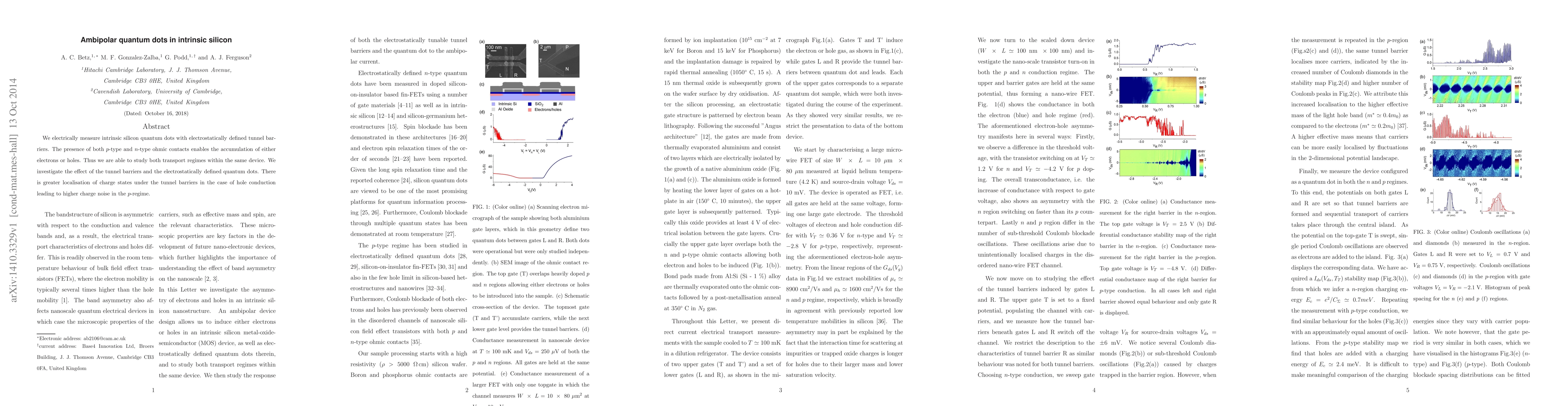
Publication
Metrics
AI Quick Summary
This study electrically measures intrinsic silicon quantum dots with tunnel barriers, allowing for the accumulation of either electrons or holes. The results show greater charge state localization and higher charge noise in the p-regime due to hole conduction.
Paper Preview
Abstract
We electrically measure intrinsic silicon quantum dots with electrostatically defined tunnel barriers. The presence of both p-type and n-type ohmic contacts enables the accumulation of either electrons or holes. Thus we are able to study both transport regimes within the same device. We investigate the effect of the tunnel barriers and the electrostatically defined quantum dots. There is greater localisation of charge states under the tunnel barriers in the case of hole conduction leading to higher charge noise in the p-regime.
AI Key Findings
Get AI-generated insights about this paper's methodology, results, significance, and more — seven facets brought into focus.
Impact
Paper Details
PDF Preview
Key Terms
Citation Network
Current paper (gray), citations (green), references (blue)
Display is limited for performance on very large graphs.
Discussion 0