Publication
Metrics
AI Quick Summary
This paper details the fabrication and electrical characterization of depletion-mode quantum dots in intrinsic silicon, revealing regular Coulomb oscillations and demonstrating a method to deactivate fixed charge using deep ultraviolet light. The design avoids complex multilayer architectures and aligns with best practices from other material systems.
Paper Preview
Abstract
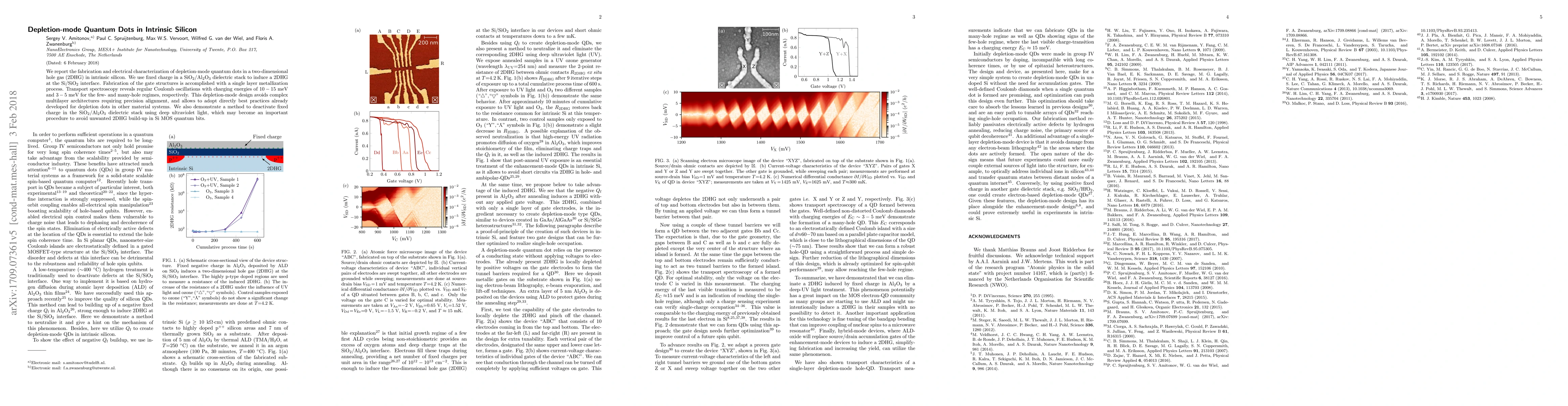
We report the fabrication and electrical characterization of depletion-mode quantum dots in a two-dimensional hole gas (2DHG) in intrinsic silicon. We use fixed charge in a SiO$_2$/Al$_2$O$_3$ dielectric stack to induce a 2DHG at the Si/SiO$_2$ interface. Fabrication of the gate structures is accomplished with a single layer metallization process. Transport spectroscopy reveals regular Coulomb oscillations with charging energies of 10-15 meV and 3-5 meV for the few- and many-hole regimes, respectively. This depletion-mode design avoids complex multilayer architectures requiring precision alignment, and allows to adopt directly best practices already developed for depletion dots in other material systems. We also demonstrate a method to deactivate fixed charge in the SiO$_2$/Al$_2$O$_3$ dielectric stack using deep ultraviolet light, which may become an important procedure to avoid unwanted 2DHG build-up in Si MOS quantum bits.
AI Key Findings
Get AI-generated insights about this paper's methodology, results, significance, and more — seven facets brought into focus.
Impact
Paper Details
PDF Preview
Key Terms
Citation Network
Current paper (gray), citations (green), references (blue)
Display is limited for performance on very large graphs.
Discussion 0