Summary
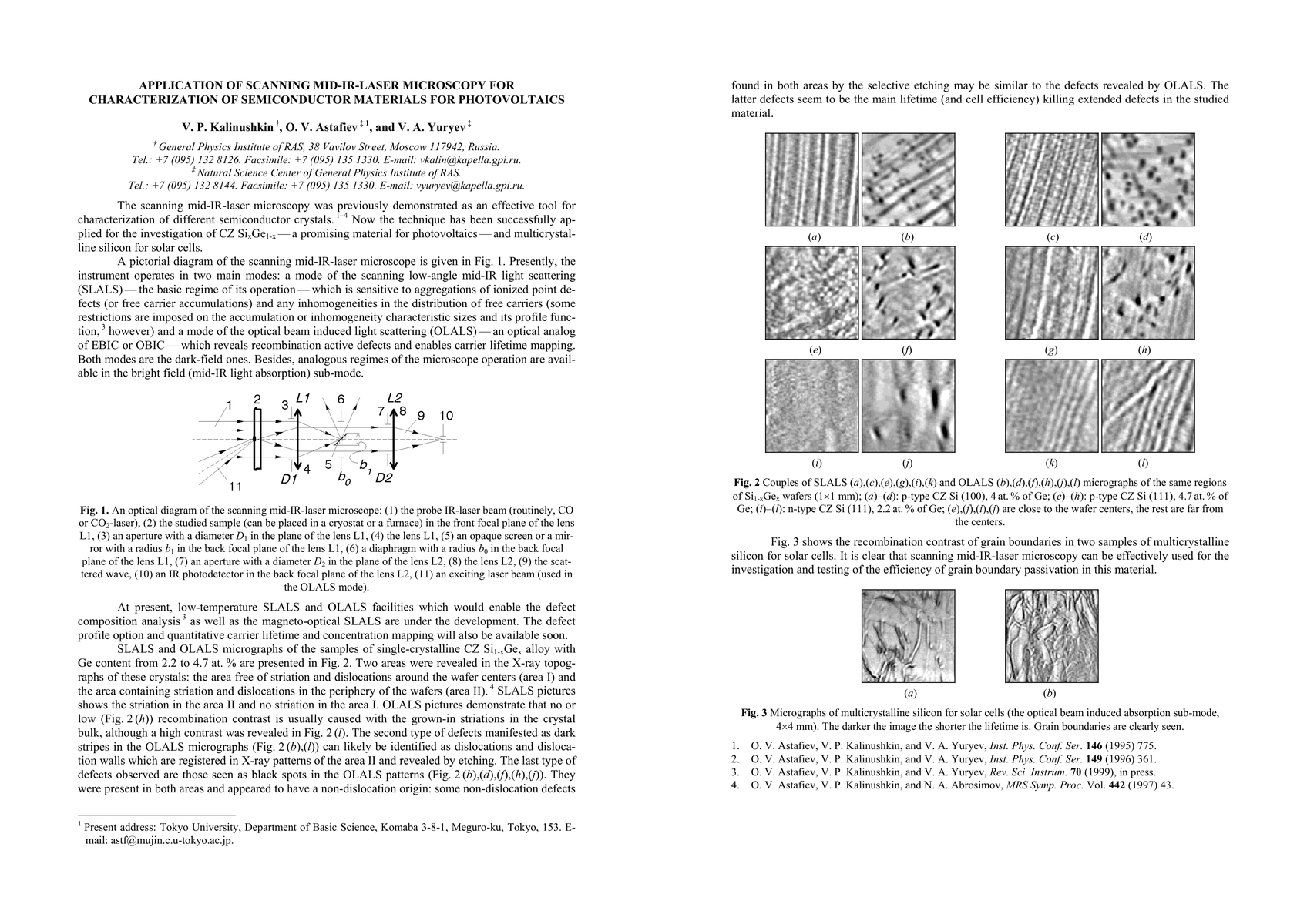
The scanning mid-IR-laser microscopy was previously demonstrated as an effective tool for characterization of different semiconductor crystals. Now the technique has been successfully applied for the investigation of CZ Si$_x$Ge$_{1-x}$---a promising material for photovoltaics---and multicrystalline silicon for solar cells.
AI Key Findings
Get AI-generated insights about this paper's methodology, results, and significance.
Paper Details
PDF Preview
Key Terms
scanning
(0.244)
semiconductor
(0.239)
crystals
(0.238)
silicon
(0.237)
si
(0.234)
ir
(0.233)
microscopy
(0.229)
mid
(0.228)
Citation Network
Current paper (gray), citations (green), references (blue)
Display is limited for performance on very large graphs.
Current Paper
Citations
References
Click to view
Similar Papers
Found 4 papers| Title | Authors | Year | Actions |
|---|
Comments (0)