The research employs atomic layer etching (ALE) of InGaAs using sequential exposures of atomic hydrogen and oxygen gas. Ex-situ spectroscopic ellipsometry is used to observe etch rates and sample smoothness.
Atomic layer etching of InGaAs using sequential exposures of atomic hydrogen and oxygen gas
Publication
Metrics
Quick Answers
What methodology did the authors use?
The research employs atomic layer etching (ALE) of InGaAs using sequential exposures of atomic hydrogen and oxygen gas. Ex-situ spectroscopic ellipsometry is used to observe etch rates and sample smoothness. More in Methodology →
What are the key results?
An etch rate of 0.095 Å/cycle was achieved at 350 °C. — The sample remains atomically smooth after 200 cycles of ALE. More in Key Results →
Why is this work significant?
This ALE process has potential applications for III-V compound semiconductor devices, enabling precise etch control on the Angstrom scale with wafer-scale uniformity, which is crucial for high-frequency performance and yield in devices like InP HEMTs. More in Significance →
What are the main limitations?
The study did not investigate the process's effect on InAlAs barrier films. — Surface passivation schemes for exposed InAlAs need further development. More in Limitations →
Abstract
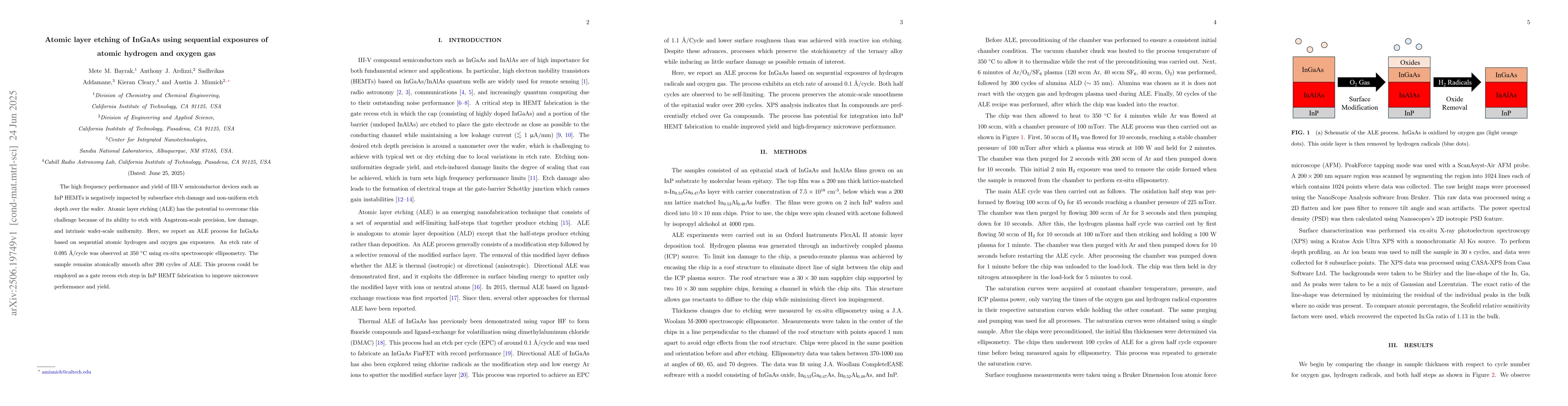
The high frequency performance and yield of III-V semiconductor devices such as InP HEMTs is negatively impacted by subsurface etch damage and non-uniform etch depth over the wafer. Atomic layer etching (ALE) has the potential to overcome this challenge because of its ability to etch with Angstrom-scale precision, low damage, and intrinsic wafer-scale uniformity. Here, we report an ALE process for InGaAs based on sequential atomic hydrogen and oxygen gas exposures. An etch rate of 0.095 \r{A}/cycle was observed at 350 {\deg}C using ex-situ spectroscopic ellipsometry. The sample remains atomically smooth after 200 cycles of ALE. This process could be employed as a gate recess etch step in InP HEMT fabrication to improve microwave performance and yield.
Key Findings, in focus
Seven facets of this paper, analysed and brought into focus by AI.
This ALE process has potential applications for III-V compound semiconductor devices, enabling precise etch control on the Angstrom scale with wafer-scale uniformity, which is crucial for high-frequency performance and yield in devices like InP HEMTs.
- An etch rate of 0.095 Å/cycle was achieved at 350 °C.
- The sample remains atomically smooth after 200 cycles of ALE.
- The process could be employed as a gate recess etch step in InP HEMT fabrication to improve microwave performance and yield.
This ALE process has potential applications for III-V compound semiconductor devices, enabling precise etch control on the Angstrom scale with wafer-scale uniformity, which is crucial for high-frequency performance and yield in devices like InP HEMTs.
The paper presents an ALE process for InGaAs with self-limiting hydrogen radical and oxygen gas exposures, demonstrating precise etch control and minimal surface damage.
This work introduces an InGaAs ALE process that combines atomic hydrogen and oxygen gas exposures, offering a scalable and uniform etching method for III-V compound semiconductor devices, which could lead to improved high-frequency performance and gain stability in InP HEMTs.
- The study did not investigate the process's effect on InAlAs barrier films.
- Surface passivation schemes for exposed InAlAs need further development.
- Investigate the process's effect on InAlAs barrier films.
- Develop surface passivation schemes for exposed InAlAs.
Impact
Authors
PDF Preview
Citation Network
Current paper (gray), citations (green), references (blue)
Display is limited for performance on very large graphs.
Discussion 0