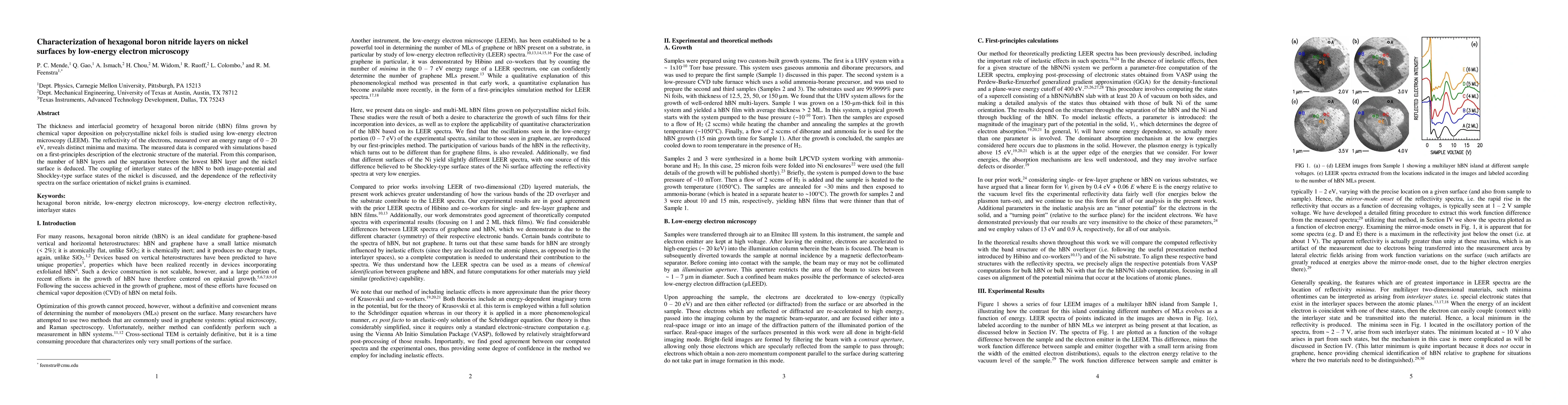
Quick Summary:

This study uses low-energy electron microscopy to characterize the thickness and interfacial geometry of hBN layers on nickel surfaces, revealing distinct electron reflectivity patterns. The analysis, combined with first-principles simulations, determines the number of hBN layers and their separation from nickel, while also discussing the coupling of hBN interlayer states with nickel surface states.

Summary

The thickness and interfacial geometry of hexagonal boron nitride (hBN) films grown by chemical vapor deposition on polycrystalline nickel foils is studied using low-energy electron microscopy (LEEM). The reflectivity of the electrons, measured over an energy range of 0 - 20 eV, reveals distinct minima and maxima. The measured data is compared with simulations based on a first-principles description of the electronic structure of the material. From this comparison, the number of hBN layers and the separation between the lowest hBN layer and the nickel surface is deduced. The coupling of interlayer states of the hBN to both image-potential and Shockley-type surface states of the nickel is discussed, and the dependence of the reflectivity spectra on the surface orientation of nickel grains is examined.

AI Key Findings

Get AI-generated insights about this paper's methodology, results, and significance.

Paper Details

PDF Preview

Download PDF

Key Terms

surface (0.237)
measured (0.210)
interfacial (0.194)
grains (0.187)
minima (0.184)
energy range (0.182)
electronic structure (0.181)
states (0.174)
thickness (0.173)
ev (0.171)
lowest (0.170)
microscopy (0.168)
examined (0.167)
orientation (0.167)
films (0.166)
reveals (0.153)
principles (0.153)
separation (0.151)
low energy (0.151)
energy (0.145)

Citation Network

Current paper (gray), citations (green), references (blue)

Current Paper
Citations
References
Click to view
Title Authors Year Actions
Bi-directional LEEM and eV-TEM spectroscopy on a graphene-hBN heterostack.
Peter S. Neu, E. Krasovskii, R. M. Tromp, S. J. van der Molen
2025
View Paper
Two dimensional boron nitride growth on nickel foils by plasma assisted molecular beam epitaxy from elemental B and N sources
Walter Batista-Pessoa, X. Wallart, D. Vignaud
2023
View Paper
Molecular beam epitaxial growth of multilayer 2D-boron nitride on Ni substrates from borazine and plasma-activated nitrogen
J. Hadid, I. Colambo, J. Avila, Aexandre Plaud, C. Boyaval, D. Deresmes, N. Nuns, P. Dudin, Annick Loiseau, J. Barjon, X. Wallart, D. Vignaud
2022
View Paper
Growth, domain structure, and atomic adsorption sites of hBN on the Ni(111) surface
M. Raths, C. Schott, Johannes Knippertz, M. Franke, Youzhi Lin, A. Haags, M. Aeschlimann, C. Kumpf, B. Stadtmüller
2021
View Paper
First-principle investigations of zigzag III-V nitride nanoribbons as CS2 scavengers
R. Yogi, N. Jaiswal
2021
View Paper
Heteroepitaxial growth of sp2-hybridized boron nitride multilayer on nickel substrates by CVD: the key role of the substrate orientation
H. Prévost, A. Andrieux-Ledier, N. Dorval, F. Fossard, J. Mérot, L. Schué, A. Plaud, E. Héripré, J. Barjon, Annick Loiseau
2020
View Paper
In Situ Monitoring of Growth of Vertically Stacked h-BN/Graphene Heterostructures on Ni Substrates and Their Interface Interaction
Wei Wei, Guanhua Zhang, Jiaqi Pan, Yi Cui, Q. Fu
2020
View Paper
First-principle investigations of Cl decorated armchair GaN nanoribbons
R. Yogi, N. Jaiswal
2020
View Paper
Dynamic observation of in-plane h-BN/graphene heterostructures growth on Ni(111)
Wei Wei, Jiaqi Pan, C. Euaruksakul, Yang Yang, Yi Cui, Q. Fu, X. Bao
2020
View Paper
Synthesis and stacking sequence characterization of h-BN/graphene heterostructures on Cu–Ni alloy
Guangyuan Lu, Guanhua Zhang, Julong Sun, Xiujun Wang, Zhiyuan Shi, D. Jiang, Haomin Wang, Ang Li, Tianru Wu, Qingkai Yu, Xiaoming Xie
2019
View Paper
Effect of Near‐Surface Dopants on the Epitaxial Growth of h‐BN on Metal Surfaces
Wei Wei, Le Lin, Guanhua Zhang, X. Ye, R. Bin, Caixia Meng, Yanxiao Ning, Q. Fu, X. Bao
2019
View Paper
Hexagonal boron nitride monolayers on metal supports: Versatile templates for atoms, molecules and nanostructures
W. Auwärter
2019
View Paper
Tuning the morphology and chemical composition of MoS2 nanostructures
G. Radovsky, Tom Shalev, A. Ismach
2019
View Paper
Cross-sectional transmission electron microscopy studies of boron ion implantation in hexagonal boron nitride
E. Aradi, S. Naidoo, F. Cummings, I. Motochi, T. Derry
2019
View Paper
Flatlands in the Holy Land: The Evolution of Layered Materials Research in Israel
O. Hod, M. Urbakh, D. Naveh, M. Bar‐Sadan, A. Ismach
2018
View Paper
Enhancement of the surface reactivity of zigzag boron nitride nanoribbons by chlorine gas decoration: A computational study
Kiran Kumar Surthi, B. De, J. Ramkumar, K. Kar
2018
View Paper
Substitutional mechanism for growth of hexagonal boron nitride on epitaxial graphene
P. Mende, Jun Li, R. Feenstra
2018
View Paper
Graphene like ZnO 2D structure from semiconductor to conductor behaviour by doping F
A. Yazdani, Behrad Barakati, A. Shokri
2018
View Paper
Mechanical behavior enhancement of defective graphene sheet employing boron nitride coating via atomistic study
A. Setoodeh, H. Badjian
2017
View Paper
Carbon-assisted chemical vapor deposition of hexagonal boron nitride
A. Ismach, H. Chou, P. Mende, A. Dolocan, R. Addou, S. Aloni, R. Wallace, R. Feenstra, R. Ruoff, L. Colombo
2017
View Paper
Spectroscopy with the Low Energy Electron Microscope
R. Tromp
2019
View Paper

Comments (0)

This website uses cookies to ensure you get the best experience. Learn more