Publication
Metrics
AI Quick Summary
This paper investigates the charge separation and photoresponse in mixed-dimensional Si nanowire/MoS2 heterojunctions, demonstrating significantly faster response times (1 us) compared to planar Si/MoS2 devices due to the enhanced exciton dissociation in the p-n heterojunction. Finite element simulations provide insights into the electrostatics influencing charge transport, guiding the design of future vdW heterojunction devices.
Paper Preview
Abstract
Layered two-dimensional (2-D) semiconductors can be combined with other low-dimensional semiconductors to form non-planar mixed-dimensional van der Waals (vdW) heterojunctions whose charge transport behavior is influenced by the heterojunction geometry, providing a new degree of freedom to engineer device functions. Towards that end, we investigated the photoresponse of Si nanowire/MoS2 heterojunction diodes with scanning photocurrent microscopy and time-resolved photocurrent measurements. Comparison of n-Si/MoS2 isotype heterojunctions with p-Si/MoS2 heterojunction diodes under varying biases shows that the depletion region in the p-n heterojunction promotes exciton dissociation and carrier collection. We measure an instrument limited response time of 1 us, which is 10 times faster than previously reported response times for planar Si/MoS2 devices, highlighting the advantages of the 1-D/2-D heterojunction. Finite element simulations of device models provide a detailed understanding of how the electrostatics affect charge transport in nanowire/vdW heterojunctions and inform the design of future vdW heterojunction photodetectors and transistors.
AI Key Findings
Get AI-generated insights about this paper's methodology, results, significance, and more — seven facets brought into focus.
Impact
Paper Details
PDF Preview
Key Terms
Citation Network
Current paper (gray), citations (green), references (blue)
Display is limited for performance on very large graphs.
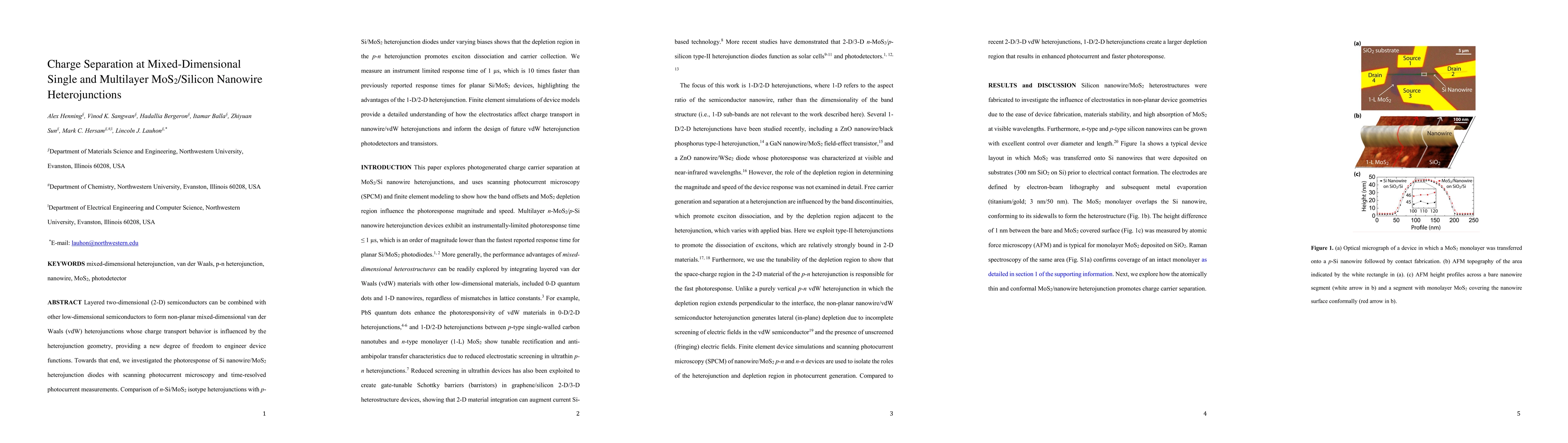
Discussion 0