Contacts to Low-Dimensional Semiconductors: Physical Theory and Analytical Model
Publication
Metrics
AI Quick Summary
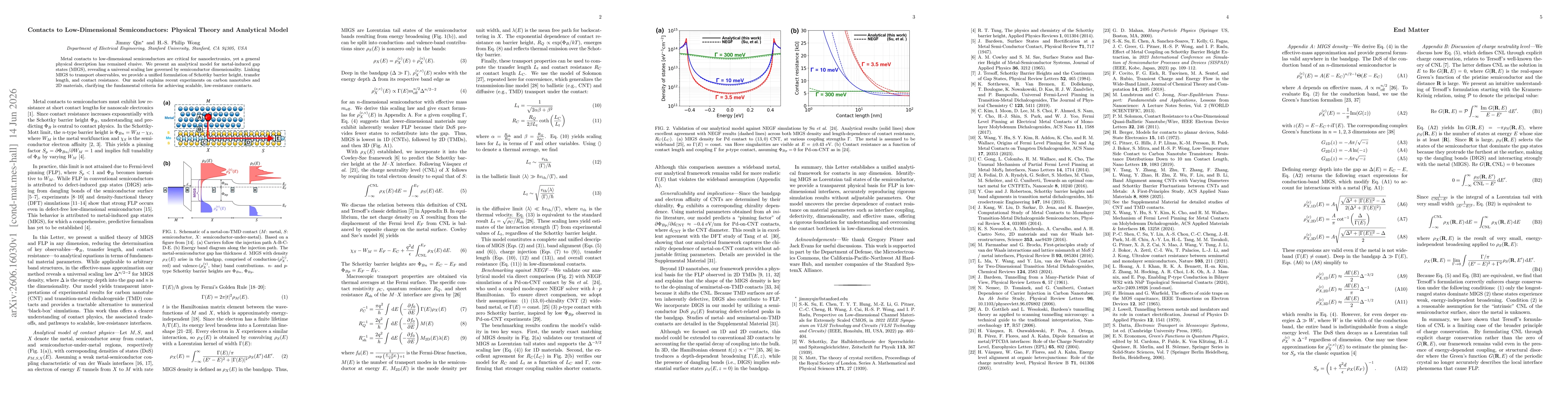
The paper develops an analytical model for metal-induced gap states (MIGS) in low-dimensional semiconductors, showing a universal scaling law dictated by dimensionality. By linking MIGS to measurable transport properties, the work unifies how Schottky barrier height, transfer length, and contact resistance behave, explaining recent experiments on carbon nanotubes and 2D materials and guiding design of scalable, low-resistance electronic contacts.
Paper Preview
Abstract
Metal contacts to low-dimensional semiconductors are critical for nanoelectronics, yet a general physical description has remained elusive. We present an analytical model for metal-induced gap states (MIGS), revealing a universal scaling law governed by semiconductor dimensionality. Linking MIGS to transport observables, we provide a unified formulation of Schottky barrier height, transfer length, and contact resistance. Our model explains recent experiments on carbon nanotubes and 2D materials, clarifying the fundamental criteria for achieving scalable, low-resistance contacts.
AI Key Findings
Get AI-generated insights about this paper's methodology, results, significance, and more — seven facets brought into focus.
Discussion 0