Publication
Metrics
AI Quick Summary
This paper details the creation of a graphene photodetector integrated into a silicon slot-waveguide to form a pn-junction, achieving high responsivity and bandwidth. The device shows a photo-thermoelectric effect at zero bias and enhanced photoconductive performance under bias, reaching a 3 dB-bandwidth of 65 GHz.
Paper Preview
Abstract
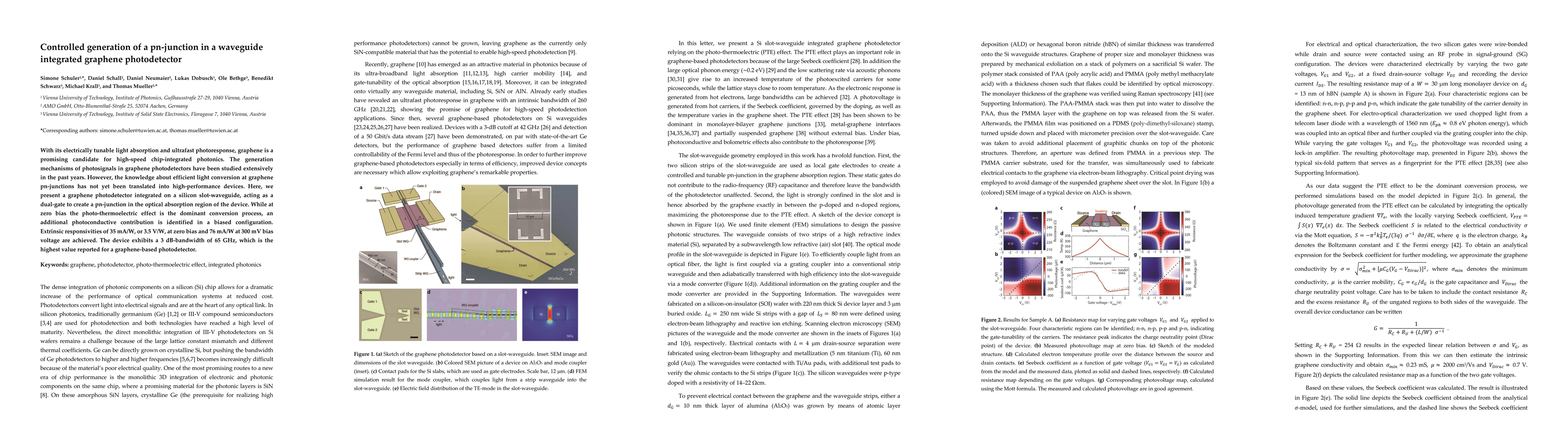
With its electrically tunable light absorption and ultrafast photoresponse, graphene is a promising candidate for high-speed chip-integrated photonics. The generation mechanisms of photosignals in graphene photodetectors have been studied extensively in the past years. However, the knowledge about efficient light conversion at graphene pn-junctions has not yet been translated into high-performance devices. Here, we present a graphene photodetector integrated on a silicon slot-waveguide, acting as a dual-gate to create a pn-junction in the optical absorption region of the device. While at zero bias the photo-thermoelectric effect is the dominant conversion process, an additional photoconductive contribution is identified in a biased configuration. Extrinsic responsivities of 35 mA/W, or 3.5 V/W, at zero bias and 76 mA/W at 300 mV bias voltage are achieved. The device exhibits a 3 dB-bandwidth of 65 GHz, which is the highest value reported for a graphene-based photodetector.
AI Key Findings
Get AI-generated insights about this paper's methodology, results, significance, and more — seven facets brought into focus.
Impact
Paper Details
PDF Preview
Key Terms
Citation Network
Current paper (gray), citations (green), references (blue)
Display is limited for performance on very large graphs.
Discussion 0