Publication
Metrics
AI Quick Summary
This research presents a graphene photodetector integrated on a silicon photonic crystal defect waveguide for telecom applications, achieving a photoresponsivity of 4.7 V/W and a bandwidth of 18 GHz. The waveguide enhances light-matter interaction and optimizes photo-thermoelectric conversion via split-gate electrodes creating a pn-junction.
Paper Preview
Abstract
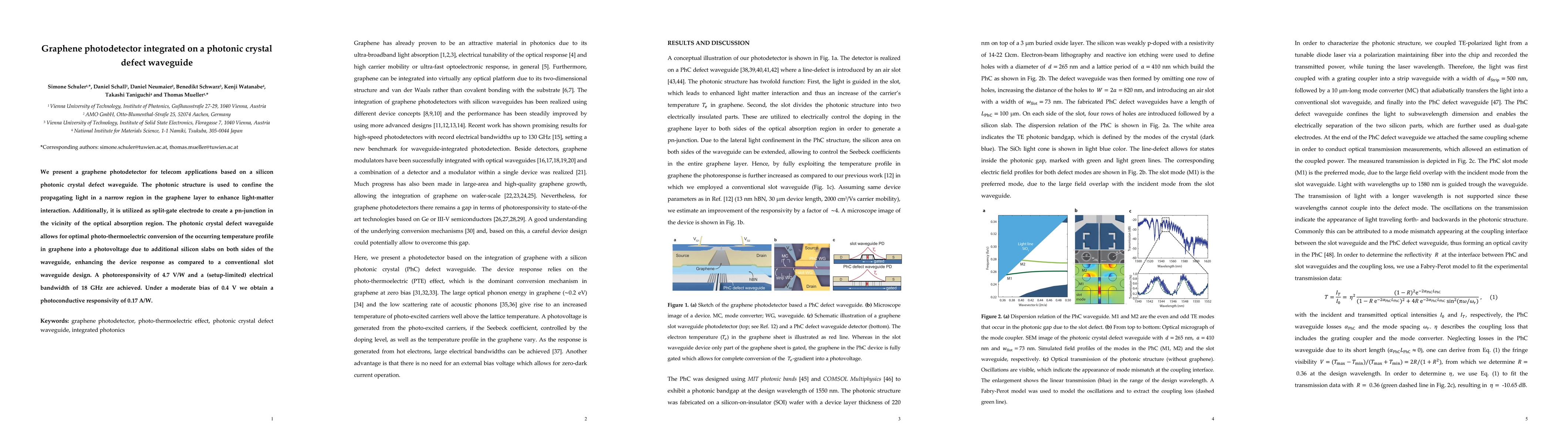
We present a graphene photodetector for telecom applications based on a silicon photonic crystal defect waveguide. The photonic structure is used to confine the propagating light in a narrow region in the graphene layer to enhance light-matter interaction. Additionally, it is utilized as split-gate electrode to create a pn-junction in the vicinity of the optical absorption region. The photonic crystal defect waveguide allows for optimal photo-thermoelectric conversion of the occurring temperature profile in graphene into a photovoltage due to additional silicon slabs on both sides of the waveguide, enhancing the device response as compared to a conventional slot waveguide design. A photoresponsivity of 4.7 V/W and a (setup-limited) electrical bandwidth of 18 GHz are achieved. Under a moderate bias of 0.4 V we obtain a photoconductive responsivity of 0.17 A/W.
AI Key Findings
Get AI-generated insights about this paper's methodology, results, significance, and more — seven facets brought into focus.
Impact
Paper Details
PDF Preview
Key Terms
Citation Network
Current paper (gray), citations (green), references (blue)
Display is limited for performance on very large graphs.
Discussion 0