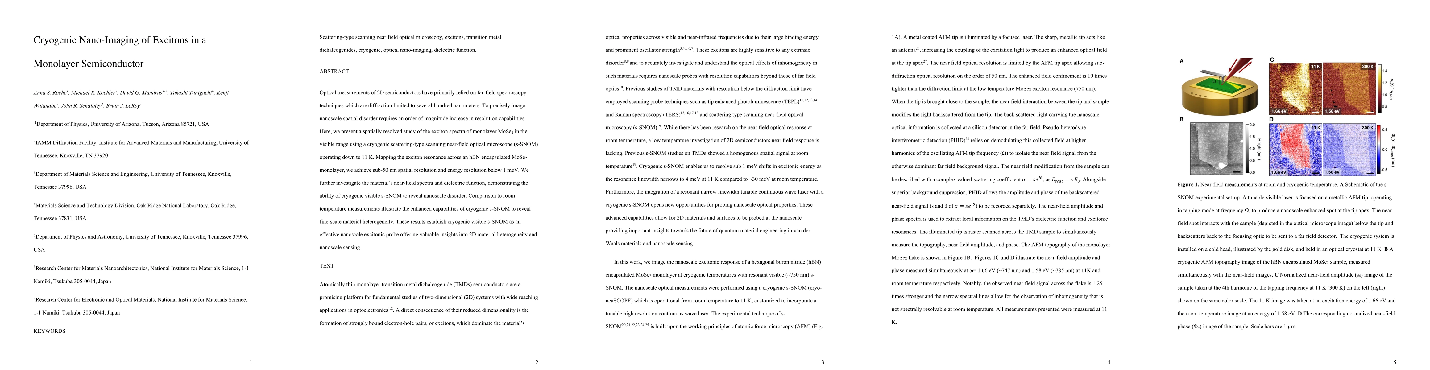
Excitons, Coulomb bound electron-hole pairs, dominate the optical response of
two-dimensional semiconductors across near-infrared and visible frequencies due
to their large binding energy and prominent oscillator strength. Previous
measurements of excitons in 2D semiconductors have primarily relied on
far-field optical spectroscopy techniques which are diffraction limited to
several hundred nanometers. To precisely image nanoscale spatial disorder
requires an order of magnitude increase in resolution capabilities. Here, we
present a study of the exciton spectra of monolayer MoSe2 in the visible range
using a cryogenic scattering-type scanning near field optical microscope
(s-SNOM) operating down to 11 K. By mapping the spatial variation in the
exciton resonance across an hBN encapsulated MoSe2 monolayer, we achieve sub-50
nm spatial resolution and energy resolution below 1 meV. We further investigate
the material's near-field spectra and dielectric function, demonstrating the
ability of cryogenic visible s-SNOM to reveal nanoscale disorder. Comparison to
room temperature measurements illustrate the enhanced capabilities of cryogenic
s-SNOM to reveal fine-scale material heterogeneity.
Discussion 0