Academic Profile
Statistics
Similar Authors
Papers on arXiv
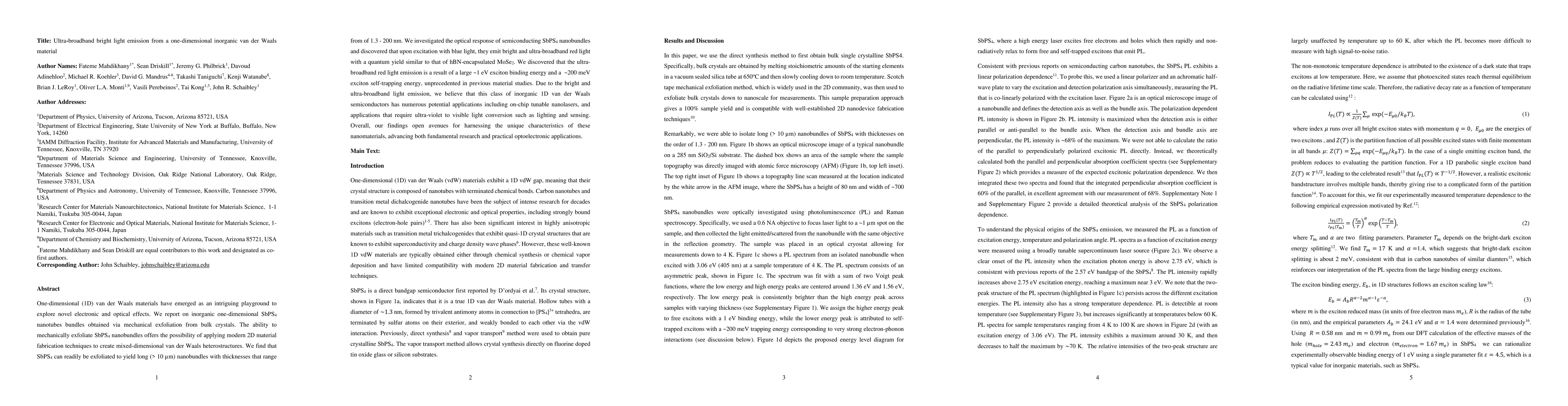
One-dimensional (1D) van der Waals materials have emerged as an intriguing playground to explore novel electronic and optical effects. We report on inorganic one-dimensional SbPS4 nanotubes bundles ...
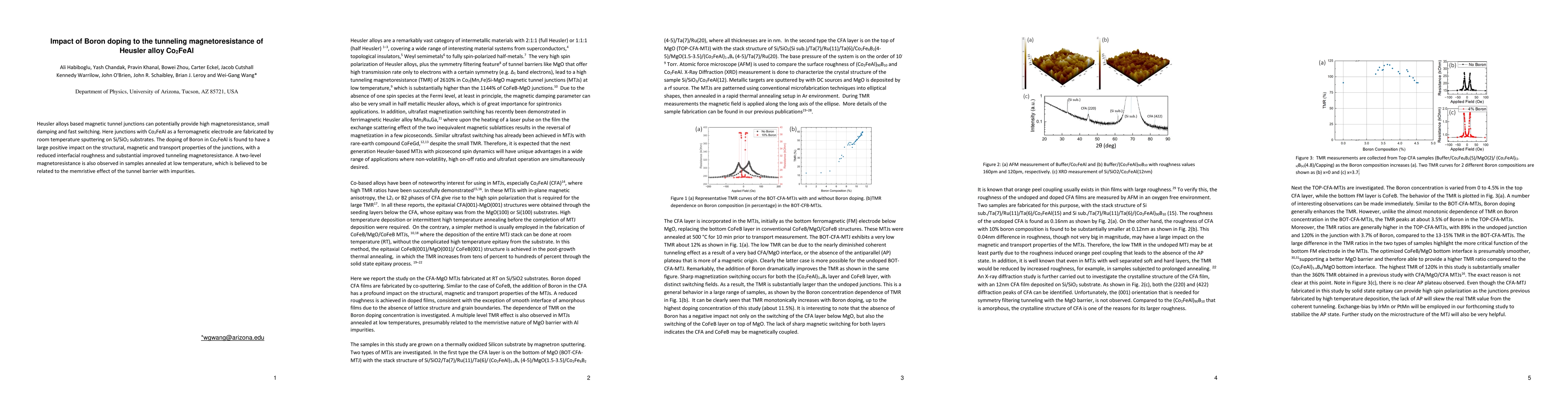
Heusler alloys based magnetic tunnel junctions can potentially provide high magnetoresistance, small damping and fast switching. Here junctions with Co2FeAl as a ferromagnetic electrode are fabricat...
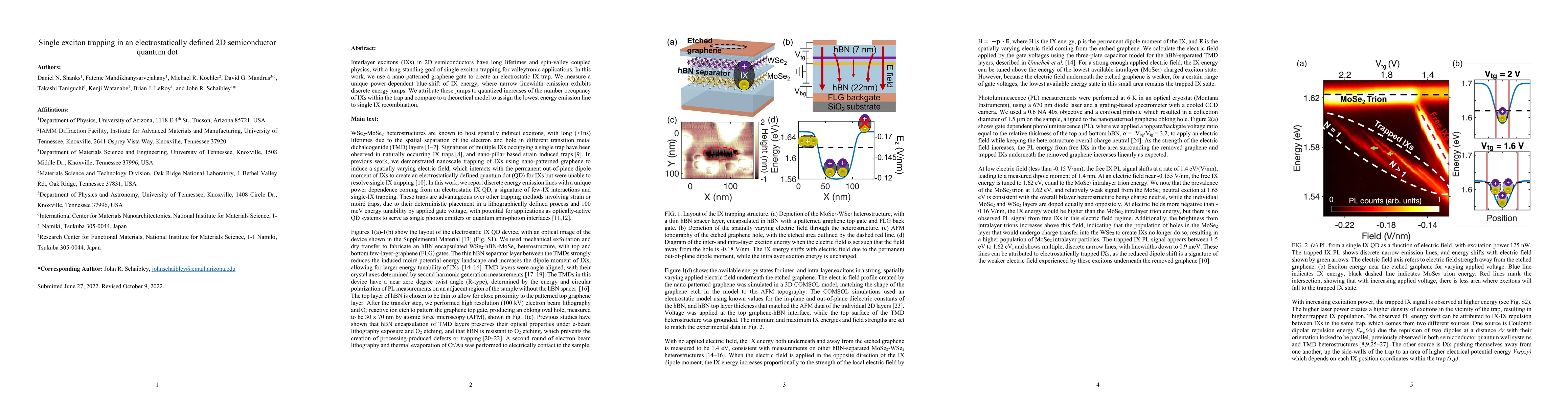
Interlayer excitons (IXs) in 2D semiconductors have long lifetimes and spin-valley coupled physics, with a long-standing goal of single exciton trapping for valleytronic applications. In this work, ...
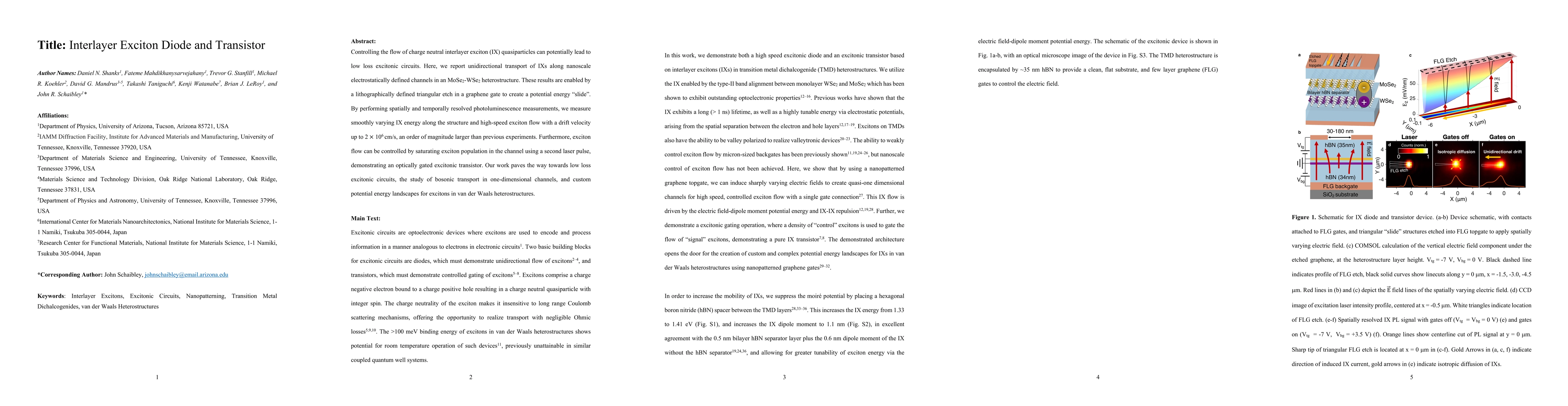
Controlling the flow of charge neutral interlayer exciton (IX) quasiparticles can potentially lead to low loss excitonic circuits. Here, we report unidirectional transport of IXs along nanoscale ele...
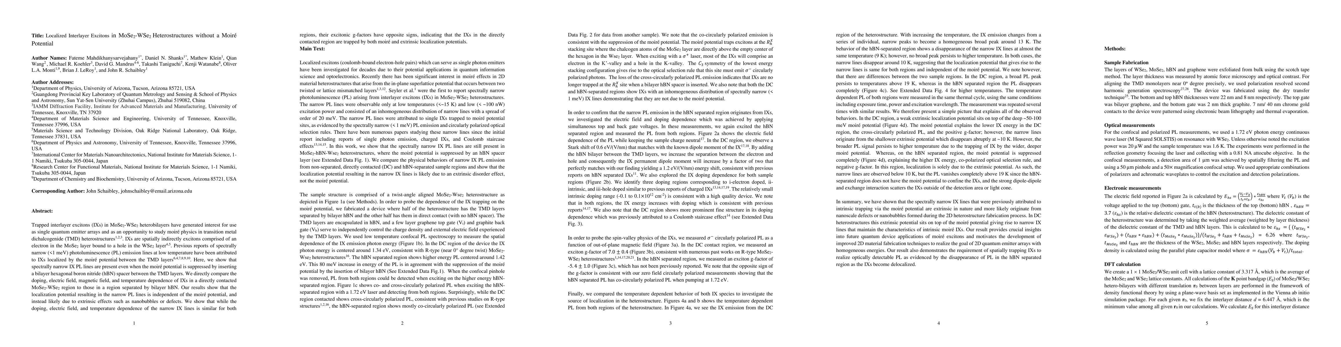
Trapped interlayer excitons (IXs) in MoSe2-WSe2 heterobilayers have generated interest for use as single quantum emitter arrays and as an opportunity to study moir\'e physics in transition metal dic...
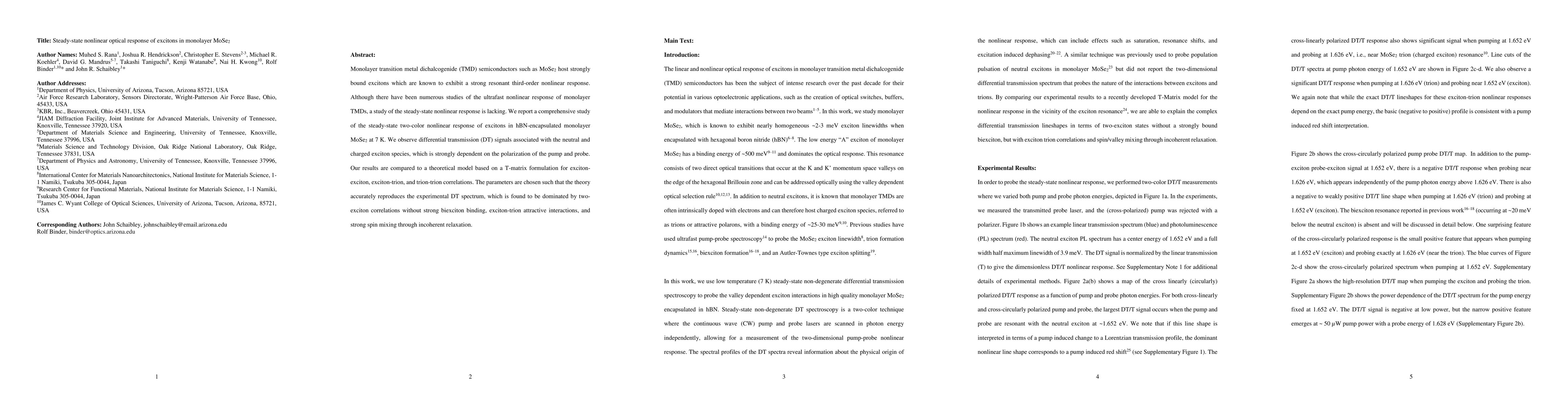
Monolayer transition metal dichalcogenide (TMD) semiconductors such as MoSe$_2$ host strongly bound excitons which are known to exhibit a strong resonant third-order nonlinear response. Although the...
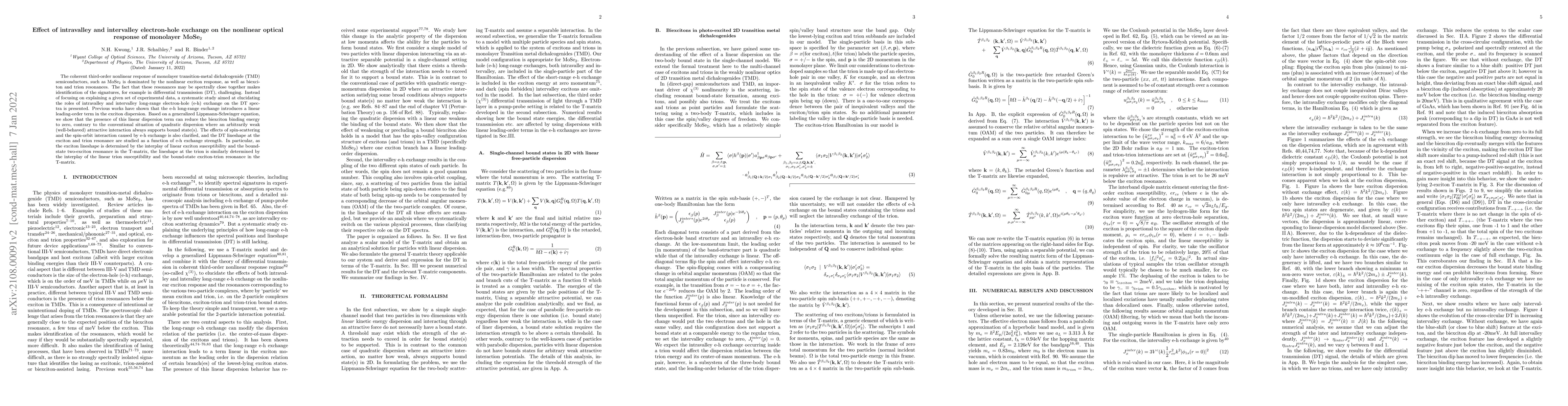
The coherent third-order nonlinear response of monolayer transition-metal dichalcogenide (TMD) semiconductors, such as MoSe$_2$ is dominated by the nonlinear exciton response, as well as biexciton a...
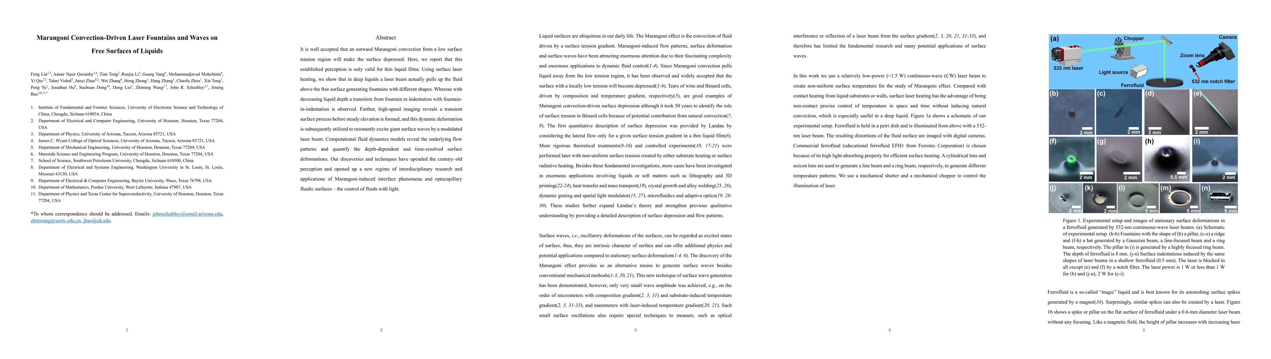
It is well accepted that an outward Marangoni convection from a low surface tension region will make the surface depressed. Here, we report that this established perception is only valid for thin li...
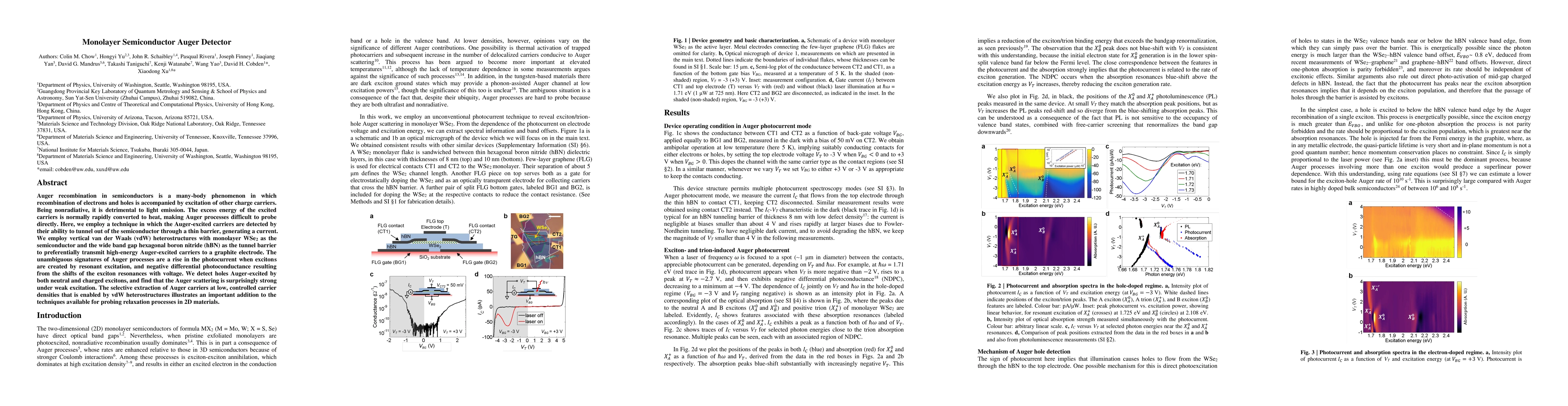
Auger recombination in semiconductors is a many-body phenomenon in which recombination of electrons and holes is accompanied by excitation of other charge carriers. Being nonradiative, it is detrime...
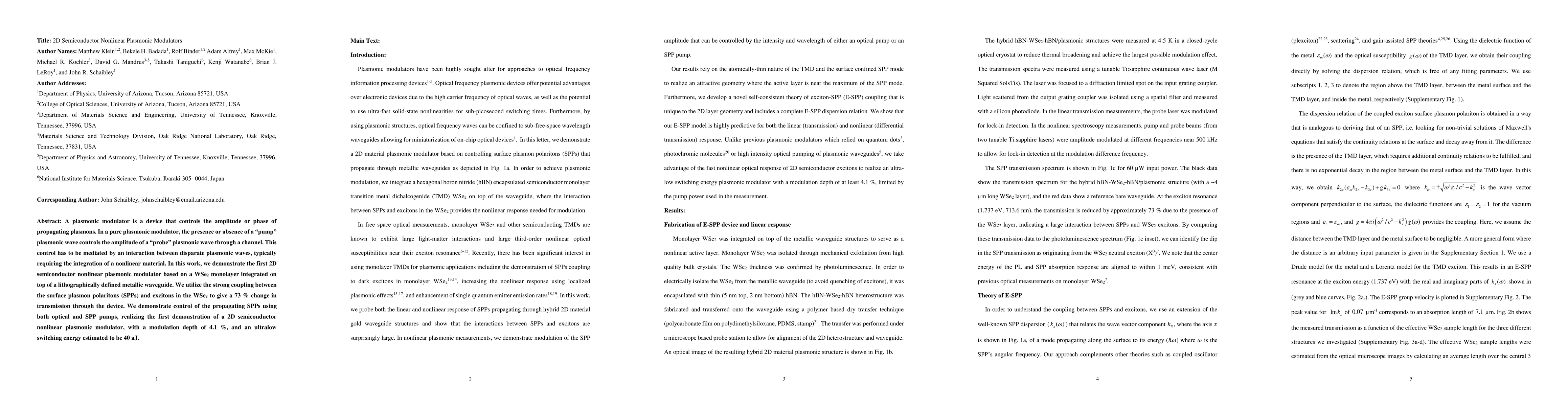
A plasmonic modulator is a device that controls the amplitude or phase of propagating plasmons. In a pure plasmonic modulator, the presence or absence of a pump plasmonic wave controls the amplitude...
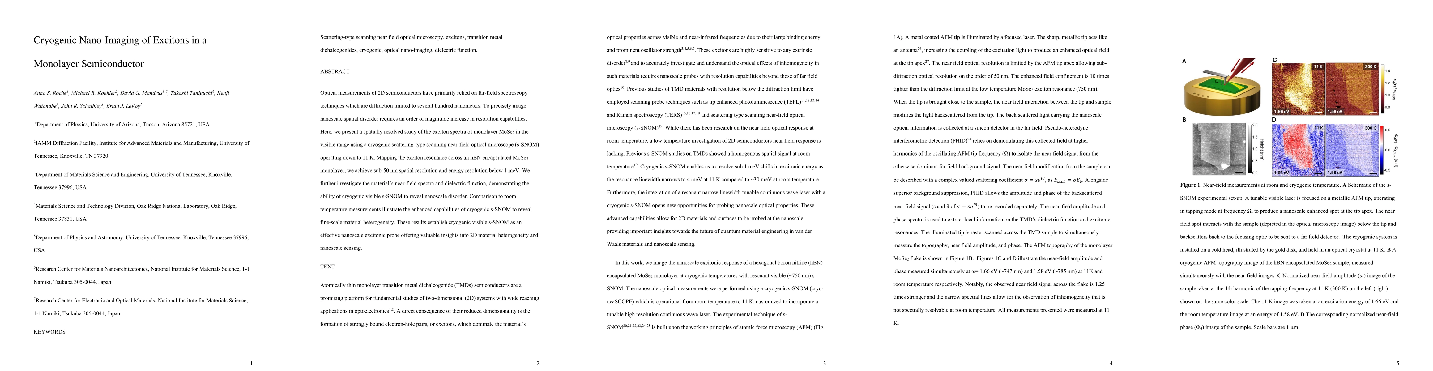
Excitons, Coulomb bound electron-hole pairs, dominate the optical response of two-dimensional semiconductors across near-infrared and visible frequencies due to their large binding energy and prominen...
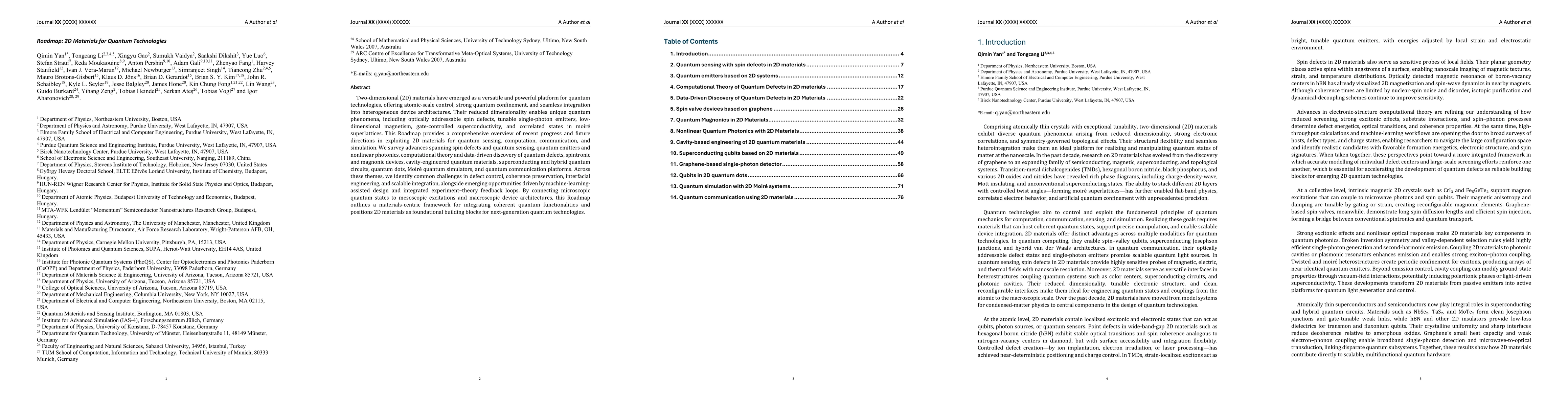
Two-dimensional (2D) materials have emerged as a versatile and powerful platform for quantum technologies, offering atomic-scale control, strong quantum confinement, and seamless integration into hete...
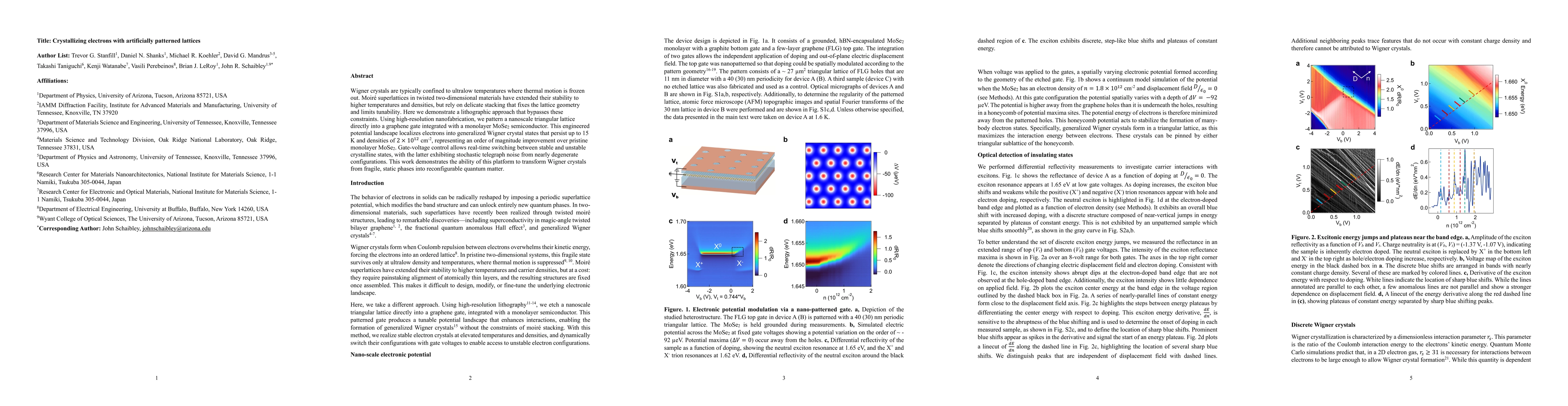
Wigner crystals are typically confined to ultralow temperatures where thermal motion is frozen out. Moiré superlattices in twisted two-dimensional materials have extended their stability to higher tem...