Publication

Published: Jan 22, 2026
Categories: cond-mat.mtrl-sci

Metrics

Source: ArXiv

Quick Actions

View PDF

Quick Answers

What methodology did the authors use?

The study employs chemical vapor deposition (CVD) to grow bilayer MoS2 films, integrating optoelectronic synaptic devices for arithmetic computing and image recognition. The devices are characterized using electrical and optical measurements, including EPSC analysis and capacitance-voltage profiling. More in Methodology →

What are the key results?

Bilayer MoS2 optoelectronic synapses demonstrate energy-efficient synaptic operations with 280 fJ per synaptic event. — The devices exhibit stable EPSC signals with ~3% cycle-to-cycle variation under optical and electrical stimuli. More in Key Results →

Why is this work significant?

This research advances neuromorphic computing by providing energy-efficient, optically controllable synaptic devices that mimic biological neural networks, with potential applications in AI and edge computing. More in Significance →

What are the main limitations?

Limited scalability of CVD-grown MoS2 films for large-scale integration. — The study focuses on specific synaptic operations, requiring further exploration of complex neural network functionalities. More in Limitations →

Paper Preview

Abstract

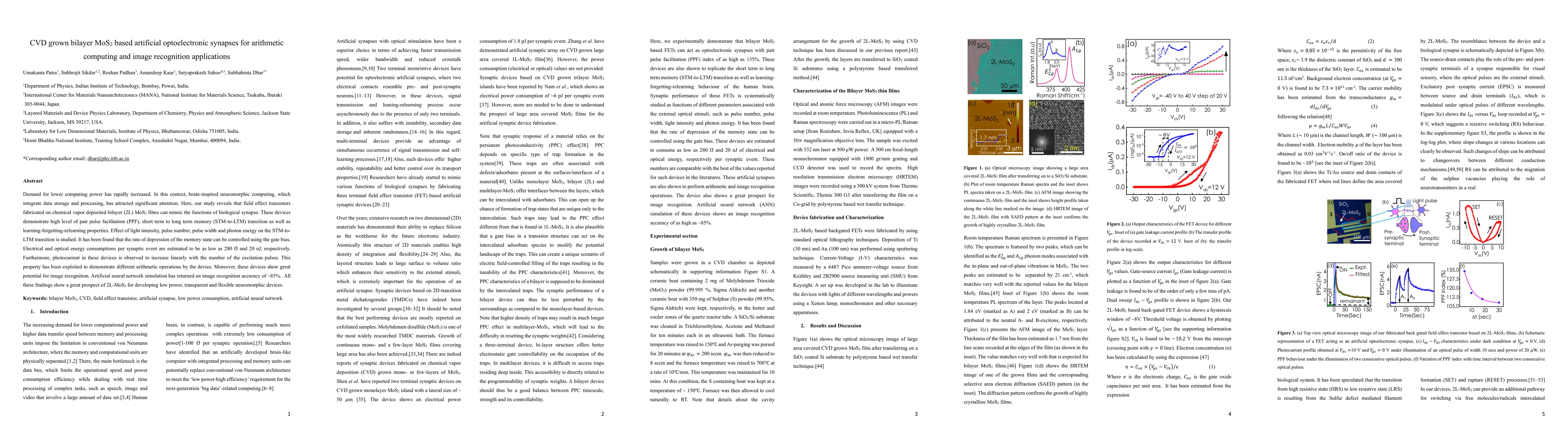
Demand for lower computing power has rapidly increased. In this context, brain-inspired neuromorphic computing, which integrate data storage and processing, has attracted significant attention. Here, our study reveals that field effect transistors fabricated on chemical vapor deposited bilayer (2L) MoS2 films can mimic the functions of biological synapse. These devices demonstrate high level of pair pulse facilitation (PPF), short term to long term memory (STM-to-LTM) transition as well as learning-forgetting-relearning properties. Effect of light intensity, pulse number, pulse width and photon energy on the STM-to-LTM transition is studied. It has been found that the rate of depression of the memory state can be controlled using the gate bias. Electrical and optical energy consumptions per synaptic event are estimated to be as low as 280 fJ and 20 nJ, respectively. Furthermore, photocurrent in these devices is observed to increase linearly with the number of the excitation pulses. This property has been exploited to demonstrate different arithmetic operations by the device. Moreover, these devices show great potential for image recognition. Artificial neural network simulation has returned an image recognition accuracy of ~85%. All these findings show a great prospect of 2L-MoS2 for developing low power, transparent and flexible neuromorphic devices.

AI Key Findings

Generated Jan 23, 2026

Methodology — What approach did the authors take?

The study employs chemical vapor deposition (CVD) to grow bilayer MoS2 films, integrating optoelectronic synaptic devices for arithmetic computing and image recognition. The devices are characterized using electrical and optical measurements, including EPSC analysis and capacitance-voltage profiling.

Key Results — What are the main findings?

  • Bilayer MoS2 optoelectronic synapses demonstrate energy-efficient synaptic operations with 280 fJ per synaptic event.
  • The devices exhibit stable EPSC signals with ~3% cycle-to-cycle variation under optical and electrical stimuli.
  • The heterosynaptic plasticity enables competitive Hebbian learning through spike-timing-dependent plasticity mechanisms.

Significance — Why does this research matter?

This research advances neuromorphic computing by providing energy-efficient, optically controllable synaptic devices that mimic biological neural networks, with potential applications in AI and edge computing.

Technical Contribution — What is the technical contribution?

The technical contribution lies in the fabrication of high-uniformity optoelectronic synapse arrays and the demonstration of energy-efficient synaptic operations with optical modulation capabilities.

Novelty — What is new about this work?

The novelty includes the integration of optoelectronic synaptic functionality with arithmetic operations and the demonstration of heterosynaptic plasticity in MoS2-based devices, which is distinct from conventional memristive systems.

Limitations — What are the limitations of this study?

  • Limited scalability of CVD-grown MoS2 films for large-scale integration.
  • The study focuses on specific synaptic operations, requiring further exploration of complex neural network functionalities.

Future Work — What did the authors propose for future work?

  • Exploring 3D stacking of MoS2 layers for enhanced device density.
  • Investigating the integration of these synapses with photonic interconnects for faster data transfer.
  • Developing advanced algorithms to leverage the full potential of heterosynaptic plasticity in neuromorphic systems.

Paper Details

Paper ID: 2601.15917
Comments: 21 pages, 14 figures
Categories:
cond-mat.mtrl-sci

How to Cite This Paper

BibTeX
@article{kaur2026cvd,
  title         = {CVD grown bilayer MoS2 based artificial optoelectronic synapses for arithmetic computing and image recognition applications},
  author        = {Kaur, Amandeep and Padhan, Roshan and Sahoo, Satyaprakash and others},
  year          = {2026},
  eprint        = {2601.15917},
  archivePrefix = {arXiv},
  primaryClass  = {cond-mat.mtrl-sci},
}
APA 7
Kaur, A., Padhan, R., Sahoo, S., Dhar, S., Sikdar, S., & Patra, U. (2026). CVD grown bilayer MoS2 based artificial optoelectronic synapses for arithmetic computing and image recognition applications. arXiv. https://arxiv.org/abs/2601.15917
MLA 9
Kaur, Amandeep, et al. "CVD grown bilayer MoS2 based artificial optoelectronic synapses for arithmetic computing and image recognition applications." arXiv, 2026, arxiv.org/abs/2601.15917.

Comments (0)

This website uses cookies to ensure you get the best experience. Learn more