Detecting Band Profiles of Devices with Conductive Atomic Force Microscopy
Publication
Metrics
Paper Preview
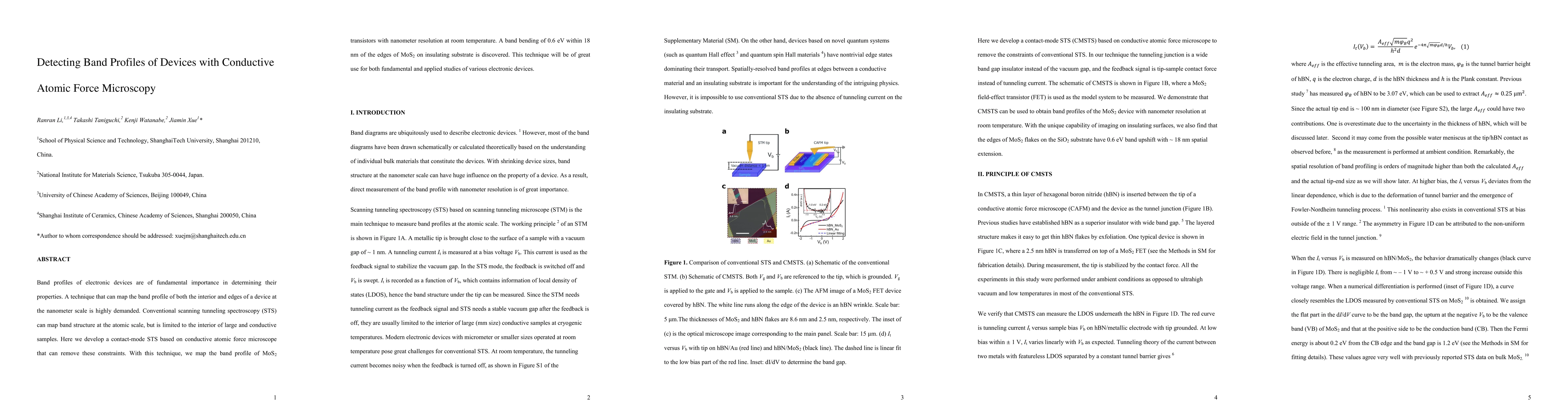
Abstract
Band profiles of electronic devices are of fundamental importance in determining their properties. A technique that can map the band profile of both the interior and edges of a device at the nanometer scale is highly demanded. Conventional scanning tunneling spectroscopy (STS) can map band structure at the atomic scale, but is limited to the interior of large and conductive samples. Here we develop a contact-mode STS based on conductive atomic force microscope that can remove these constraints. With this technique, we map the band profile of MoS$_2$ transistors with nanometer resolution at room temperature. A band bending of 0.6 eV within 18 nm of the edges of MoS$_2$ on insulating substrate is discovered. This technique will be of great use for both fundamental and applied studies of various electronic devices.
AI Key Findings
Get AI-generated insights about this paper's methodology, results, significance, and more — seven facets brought into focus.
Impact
Paper Details
Authors
PDF Preview
Key Terms
Citation Network
Current paper (gray), citations (green), references (blue)
Display is limited for performance on very large graphs.
Discussion 0