Summary
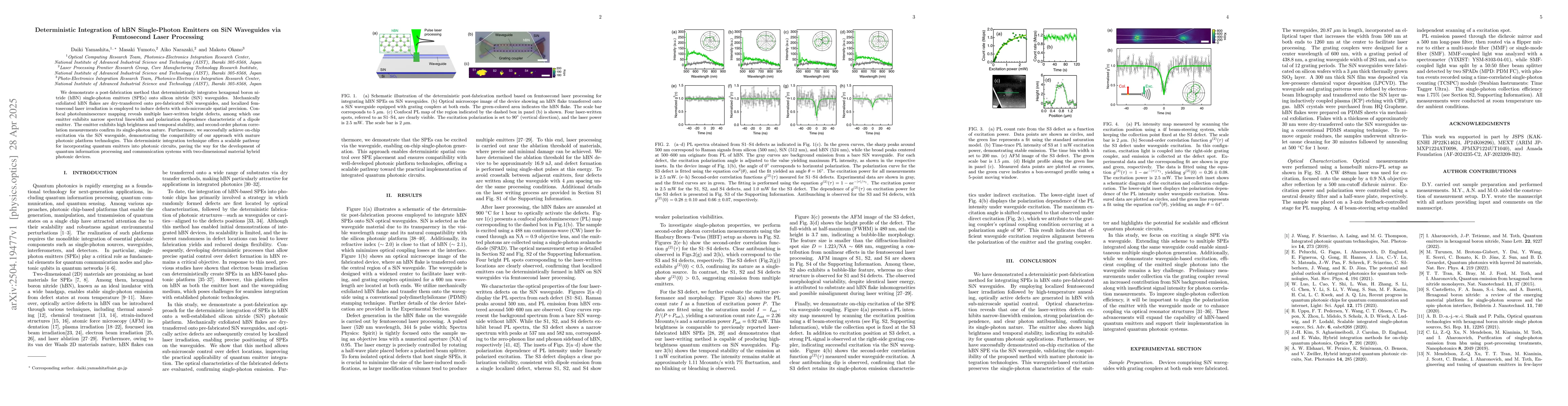
We demonstrate a post-fabrication method that deterministically integrates hexagonal boron nitride (hBN) single-photon emitters (SPEs) onto silicon nitride (SiN) waveguides. Mechanically exfoliated hBN flakes are dry-transferred onto pre-fabricated SiN waveguides, and localized femtosecond laser irradiation is employed to induce defects with sub-microscale spatial precision. Confocal photoluminescence mapping reveals multiple laser-written bright defects, among which one emitter exhibits narrow spectral linewidth and polarization dependence characteristic of a dipole emitter. The emitter exhibits high brightness and temporal stability, and second-order photon correlation measurements confirm its single-photon nature. Furthermore, we successfully achieve on-chip excitation via the SiN waveguide, demonstrating the compatibility of our approach with mature photonic platform technologies. This deterministic integration technique offers a scalable pathway for incorporating quantum emitters into photonic circuits, paving the way for the development of quantum information processing and communication systems with two-dimensional material hybrid photonic devices.
AI Key Findings
Generated Jun 08, 2025
Methodology
The method involves dry-transferring mechanically exfoliated hBN flakes onto pre-fabricated SiN waveguides, followed by localized femtosecond laser irradiation to induce defects with sub-microscale precision.
Key Results
- Demonstrated deterministic integration of hBN single-photon emitters (SPEs) onto SiN waveguides.
- Identified multiple laser-written bright defects, with one emitter showing narrow spectral linewidth and polarization dependence characteristic of a dipole emitter.
- Confirmed high brightness, temporal stability, and single-photon nature of the emitter through measurements.
Significance
This research offers a scalable pathway for incorporating quantum emitters into photonic circuits, advancing the development of quantum information processing and communication systems using two-dimensional material hybrid photonic devices.
Technical Contribution
The paper presents a novel post-fabrication method for deterministic integration of hBN SPEs onto SiN waveguides using femtosecond laser processing.
Novelty
This work introduces a new approach for integrating quantum emitters into photonic circuits, combining hBN SPEs with SiN waveguides, which is different from existing research focusing on other materials or integration techniques.
Limitations
- The paper does not discuss scalability of the method for large-scale integration.
- Potential for laser-induced damage to waveguides or emitters is not addressed.
Future Work
- Explore large-scale integration of hBN SPEs on SiN waveguides.
- Investigate long-term stability and potential degradation mechanisms of laser-induced emitters.
Paper Details
PDF Preview
Citation Network
Current paper (gray), citations (green), references (blue)
Display is limited for performance on very large graphs.
Similar Papers
Found 4 papersSilicon nitride waveguides with intrinsic single-photon emitters for integrated quantum photonics
Vladimir M. Shalaev, Alexandra Boltasseva, Alexander Senichev et al.
No citations found for this paper.
Comments (0)