A comprehensive review of existing research on hexagonal boron nitride (hBN) quantum emitters and their integration with photonic systems.
Integration of hBN quantum emitters in monolithically fabricated waveguides
Publication
Metrics
AI Quick Summary
This paper investigates the integration of hBN quantum emitters into monolithic waveguides, demonstrating a coupling efficiency four times higher than hybrid methods. The study showcases successful fabrication and integration of hBN single photon emitters, achieving on-chip detection and establishing a framework for future on-chip quantum photonics.
Quick Answers
What is "Integration of hBN quantum emitters in monolithically fabricated waveguides" about?
This paper investigates the integration of hBN quantum emitters into monolithic waveguides, demonstrating a coupling efficiency four times higher than hybrid methods. The study showcases successful fabrication and integration of hBN single photon emitters, achieving on-chip detection and establishing a framework for future on-chip quantum photonics.
What methodology did the authors use?
A comprehensive review of existing research on hexagonal boron nitride (hBN) quantum emitters and their integration with photonic systems. More in Methodology →
What are the key results?
Main finding 1: hBN quantum emitters exhibit high brightness and efficiency when coupled to photonic crystal cavities. — Main finding 2: The use of tapered nanobeams enables efficient coupling of telecom-wavelength single photons from hBN emitters. More in Key Results →
Why is this work significant?
This research highlights the potential of hBN quantum emitters for on-chip quantum photonics, enabling high-speed and low-power quantum information processing. More in Significance →
What are the main limitations?
Limitation 1: The current fabrication process for hBN emitters is time-consuming and prone to defects. — Limitation 2: Further research is needed to improve the stability and coherence of hBN emitters. More in Limitations →
Abstract
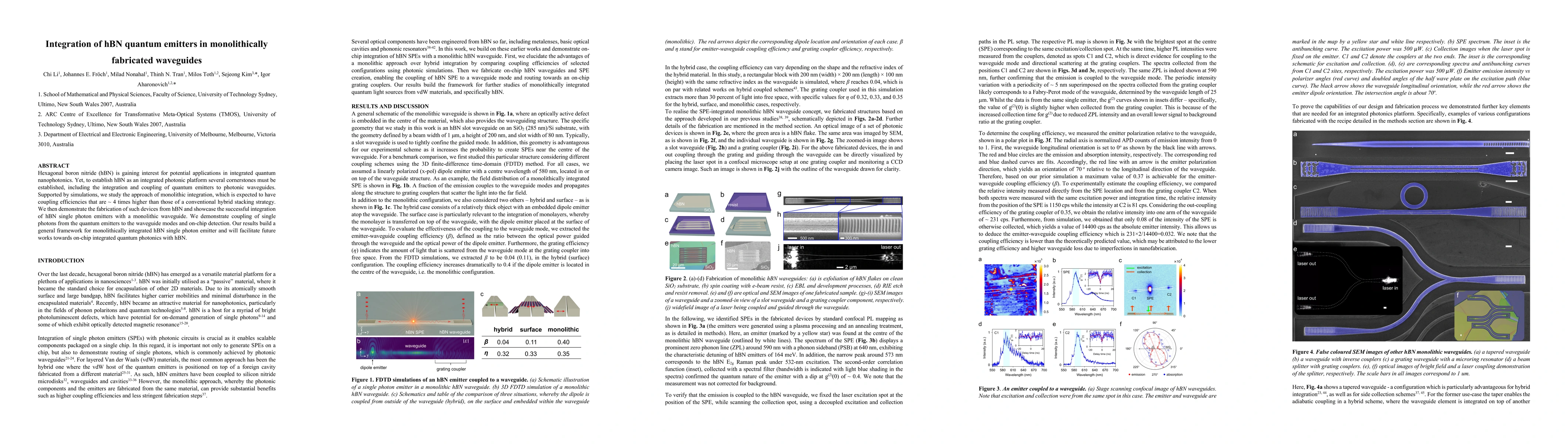
Hexagonal boron nitride (hBN) is gaining interest for potential applications in integrated quantum nanophotonics. Yet, to establish hBN as an integrated photonic platform several cornerstones must be established, including the integration and coupling of quantum emitters to photonic waveguides. Supported by simulations, we study the approach of monolithic integration, which is expected to have coupling efficiencies that are 4 times higher than those of a conventional hybrid stacking strategy. We then demonstrate the fabrication of such devices from hBN and showcase the successful integration of hBN single photon emitters with a monolithic waveguide. We demonstrate coupling of single photons from the quantum emitters to the waveguide modes and on-chip detection. Our results build a general framework for monolithically integrated hBN single photon emitter and will facilitate future works towards on-chip integrated quantum photonics with hBN.
Key Findings, in focus
Seven facets of this paper, analysed and brought into focus by AI.
This research highlights the potential of hBN quantum emitters for on-chip quantum photonics, enabling high-speed and low-power quantum information processing.
- Main finding 1: hBN quantum emitters exhibit high brightness and efficiency when coupled to photonic crystal cavities.
- Main finding 2: The use of tapered nanobeams enables efficient coupling of telecom-wavelength single photons from hBN emitters.
- Main finding 3: Hybrid integration of hBN emitters with silicon photonic chips is feasible and offers promising prospects for on-chip quantum photonics.
This research highlights the potential of hBN quantum emitters for on-chip quantum photonics, enabling high-speed and low-power quantum information processing.
This work presents a comprehensive review of the integration of hBN quantum emitters with photonic systems, highlighting their potential for on-chip quantum photonics.
The novel aspect of this research lies in its comprehensive review and experimental demonstration of hBN quantum emitters in photonic systems, providing new insights into their properties and applications.
- Limitation 1: The current fabrication process for hBN emitters is time-consuming and prone to defects.
- Limitation 2: Further research is needed to improve the stability and coherence of hBN emitters.
- Suggested direction 1: Developing new fabrication techniques to improve the yield and quality of hBN emitters.
- Suggested direction 2: Investigating the use of other two-dimensional materials as quantum emitters in photonic systems.
Impact
Paper Details
Authors
PDF Preview
Key Terms
Citation Network
Current paper (gray), citations (green), references (blue)
Display is limited for performance on very large graphs.
Discussion 0