Publication
Metrics
AI Quick Summary
This paper demonstrates the use of advanced STEM to directly image moiré patterns at the 2D/3D interface between MoS2 and Au, revealing hidden crystallographic structures. The study shows that moiré engineering can modulate charge density, suggesting potential for opto-electronic applications at such interfaces.
Paper Preview
Abstract
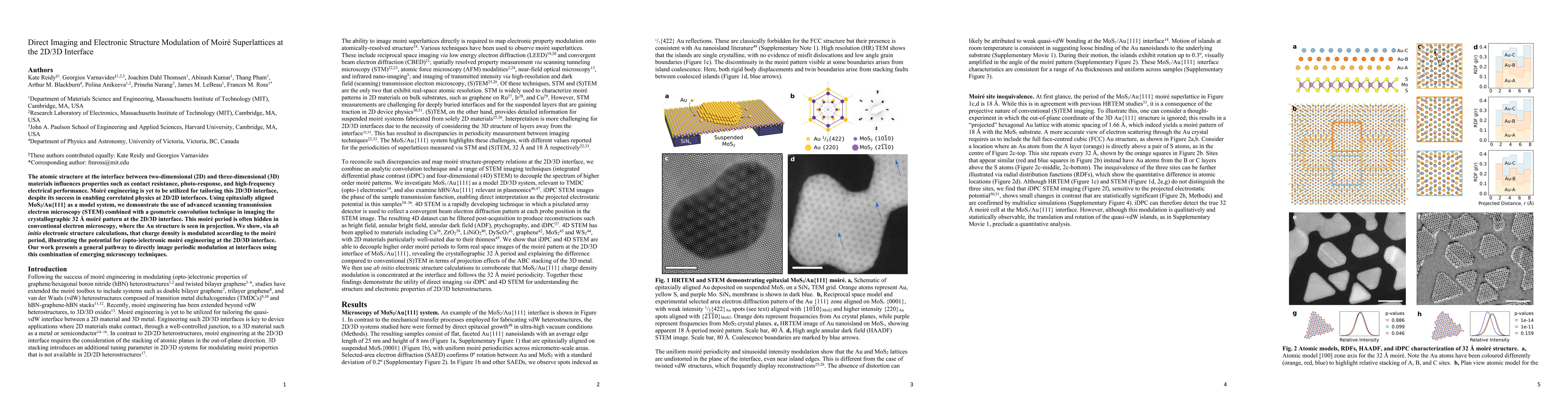
The atomic structure at the interface between two-dimensional (2D) and three-dimensional (3D) materials influences properties such as contact resistance, photo-response, and high-frequency electrical performance. Moir\'e engineering is yet to be utilized for tailoring this 2D/3D interface, despite its success in enabling correlated physics at 2D/2D interfaces. Using epitaxially aligned MoS2/Au{111} as a model system, we demonstrate the use of advanced scanning transmission electron microscopy (STEM) combined with a geometric convolution technique in imaging the crystallographic 32 A moir\'e pattern at the 2D/3D interface. This moir\'e period is often hidden in conventional electron microscopy, where the Au structure is seen in projection. We show, via ab initio electronic structure calculations, that charge density is modulated according to the moir\'e period, illustrating the potential for (opto-)electronic moir\'e engineering at the 2D/3D interface. Our work presents a general pathway to directly image periodic modulation at interfaces using this combination of emerging microscopy techniques.
AI Key Findings
Get AI-generated insights about this paper's methodology, results, significance, and more — seven facets brought into focus.
Impact
Paper Details
PDF Preview
Key Terms
Citation Network
Current paper (gray), citations (green), references (blue)
Display is limited for performance on very large graphs.
Discussion 0