Publication
Metrics
Quick Actions
AI Quick Summary
This research proposes a novel surface passivation technique using phosphine annealing to mitigate surface defects in III-As(P) photonic nanostructures, achieving an almost tenfold reduction in surface recombination velocity compared to traditional methods. The method also employs wider bandgap material encapsulation to maintain device band structure.
Quick Answers
What is "Efficient passivation of III-As(P) photonic interfaces" about?
This research proposes a novel surface passivation technique using phosphine annealing to mitigate surface defects in III-As(P) photonic nanostructures, achieving an almost tenfold reduction in surface recombination velocity compared to traditional methods. The method also employs wider bandgap material encapsulation to maintain device band structure.
What methodology did the authors use?
The research proposes a novel surface passivation approach for III-As(P) photonic nanostructures using phosphine (PH3) annealing inside an MOCVD chamber to eliminate defects induced by dry etching and subsequent oxidation. More in Methodology →
What are the key results?
An almost order of magnitude reduction in surface recombination velocity (from $2 \times 10^3 \, \mathrm{cm/s}$ for PH3 annealing compared to $1.5 \times 10^4 \, \mathrm{cm/s}$ for non-passivated structures and $5 \times 10^3 \, \mathrm{cm/s}$ for (NH4)2S wet treatment followed by Al2O3 encapsulation). — Further reduction to $5 \times 10^2 \, \mathrm{cm/s}$ achieved for InP-regrown samples. More in Key Results →
Why is this work significant?
This research is significant as it presents an efficient method to passivate III-As(P) photonic interfaces, crucial for enhancing the performance of nanophotonic and quantum photonic devices, especially as device dimensions are reduced. More in Significance →
What are the main limitations?
The study is limited to III-As(P) quantum well nanostructures and may not directly apply to other semiconductor materials. — The findings are based on specific experimental conditions and may vary under different growth or processing parameters. More in Limitations →
Abstract
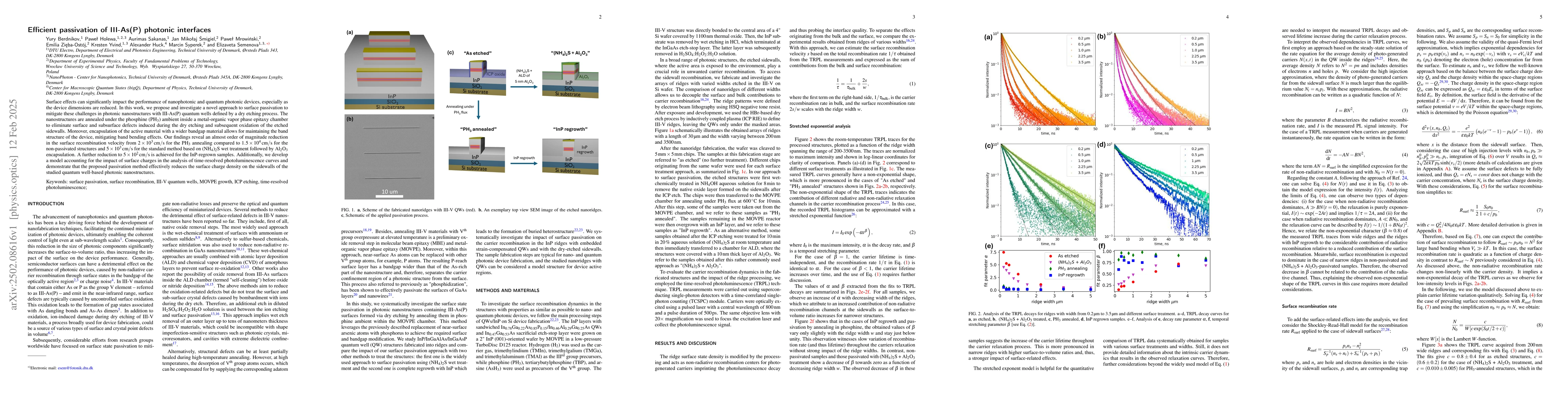
Surface effects can significantly impact the performance of nanophotonic and quantum photonic devices, especially as the device dimensions are reduced. In this work, we propose and investigate a novel approach to surface passivation to mitigate these challenges in photonic nanostructures with III-As(P) quantum wells defined by a dry etching process. The nanostructures are annealed under the phosphine (PH$_3$) ambient inside a metal-organic vapor phase epitaxy chamber to eliminate surface and subsurface defects induced during the dry etching and subsequent oxidation of the etched sidewalls. Moreover, encapsulation of the active material with a wider bandgap material allows for maintaining the band structure of the device, mitigating band bending effects. Our findings reveal an almost order of magnitude reduction in the surface recombination velocity from $2 \times 10^3 \, \mathrm{cm/s}$ for the PH$_3$ annealing compared to $1.5 \times 10^4 \, \mathrm{cm/s}$ for the non-passivated structures and $5 \times 10^3 \, \mathrm{cm/s}$ for the standard method based on (NH$_4$)$_2$S wet treatment followed by Al$_2$O$_3$ encapsulation. A further reduction to $5 \times 10^2 \, \mathrm{cm/s}$ is achieved for the InP-regrown samples. Additionally, we develop a model accounting for the impact of surface charges in the analysis of time-resolved photoluminescence curves and demonstrate that the proposed passivation method effectively reduces the surface charge density on the sidewalls of the studied quantum well-based photonic nanostructures.
AI Key Findings
Generated Jun 11, 2025
Methodology — What approach did the authors take?
The research proposes a novel surface passivation approach for III-As(P) photonic nanostructures using phosphine (PH3) annealing inside an MOCVD chamber to eliminate defects induced by dry etching and subsequent oxidation.
Key Results — What are the main findings?
- An almost order of magnitude reduction in surface recombination velocity (from $2 \times 10^3 \, \mathrm{cm/s}$ for PH3 annealing compared to $1.5 \times 10^4 \, \mathrm{cm/s}$ for non-passivated structures and $5 \times 10^3 \, \mathrm{cm/s}$ for (NH4)2S wet treatment followed by Al2O3 encapsulation).
- Further reduction to $5 \times 10^2 \, \mathrm{cm/s}$ achieved for InP-regrown samples.
- Development of a model to analyze time-resolved photoluminescence curves, demonstrating the effectiveness of the proposed passivation method in reducing surface charge density on sidewalls.
Significance — Why does this research matter?
This research is significant as it presents an efficient method to passivate III-As(P) photonic interfaces, crucial for enhancing the performance of nanophotonic and quantum photonic devices, especially as device dimensions are reduced.
Technical Contribution — What is the technical contribution?
The paper introduces a novel surface passivation technique using PH3 annealing, which effectively reduces surface and subsurface defects in III-As(P) photonic nanostructures, leading to improved device performance.
Novelty — What is new about this work?
The proposed method combines PH3 annealing with wider bandgap material encapsulation to mitigate surface recombination and band bending effects, offering a more efficient passivation approach than existing methods.
Limitations — What are the limitations of this study?
- The study is limited to III-As(P) quantum well nanostructures and may not directly apply to other semiconductor materials.
- The findings are based on specific experimental conditions and may vary under different growth or processing parameters.
Future Work — What did the authors propose for future work?
- Further investigation into the long-term stability and reliability of the proposed passivation method.
- Exploration of the method's applicability to a broader range of semiconductor materials and device architectures.
Paper Details
How to Cite This Paper
@article{huck2025efficient,
title = {Efficient passivation of III-As(P) photonic interfaces},
author = {Huck, Alexander and Sakanas, Aurimas and Semenova, Elizaveta and others},
year = {2025},
eprint = {2502.08616},
archivePrefix = {arXiv},
primaryClass = {physics.optics},
}
Huck, A., Sakanas, A., Semenova, E., Zięba-Ostój, E., Śmigiel, J., Yvind, K., Syperek, M., Holewa, P., Mrowiński, P., & Berdnikov, Y. (2025). Efficient passivation of III-As(P) photonic interfaces. arXiv. https://arxiv.org/abs/2502.08616
Huck, Alexander, et al. "Efficient passivation of III-As(P) photonic interfaces." arXiv, 2025, arxiv.org/abs/2502.08616.
PDF Preview
Similar Papers
Found 4 papersElectrodynamics of Photonic Temporal Interfaces
Emanuele Galiffi, Diego Martinez Solís, Shixiong Yin et al.
No citations found for this paper.
Comments (0)