Academic Profile
Statistics
Similar Authors
Papers on arXiv
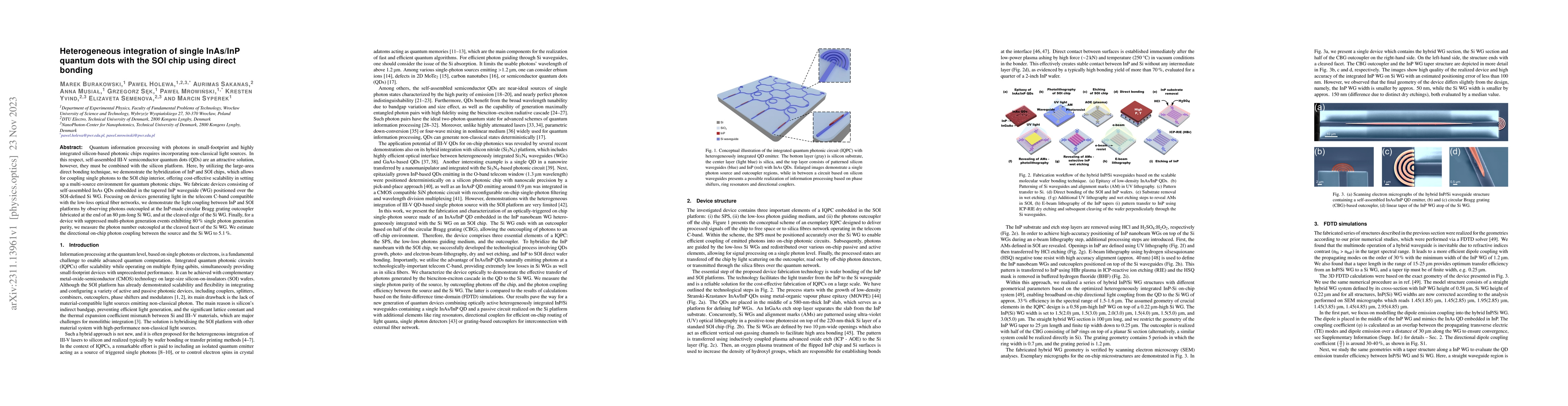
Quantum information processing with photons in small-footprint and highly integrated silicon-based photonic chips requires incorporating non-classical light sources. In this respect, self-assembled ...
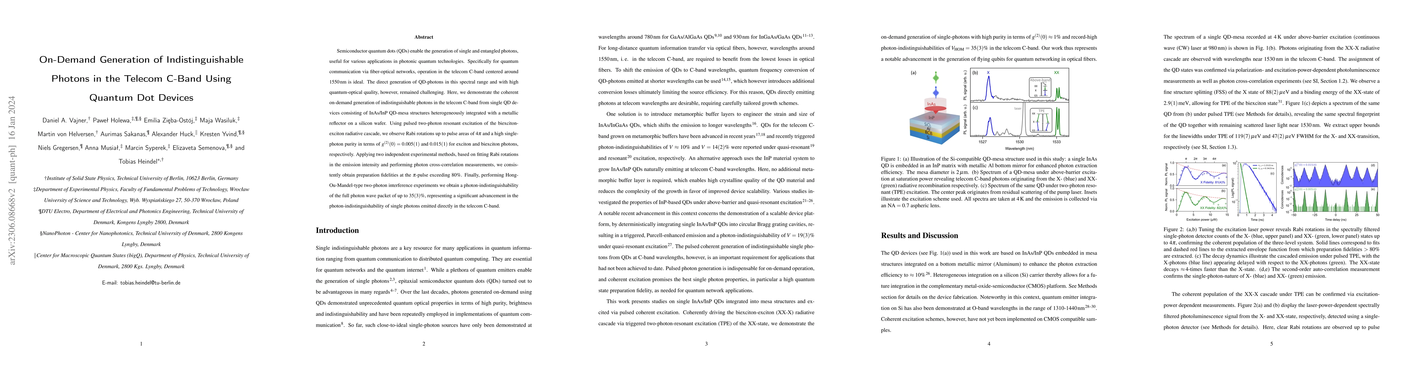
Semiconductor quantum dots (QDs) enable the generation of single and entangled photons, useful for various applications in photonic quantum technologies. Specifically for quantum communication via f...
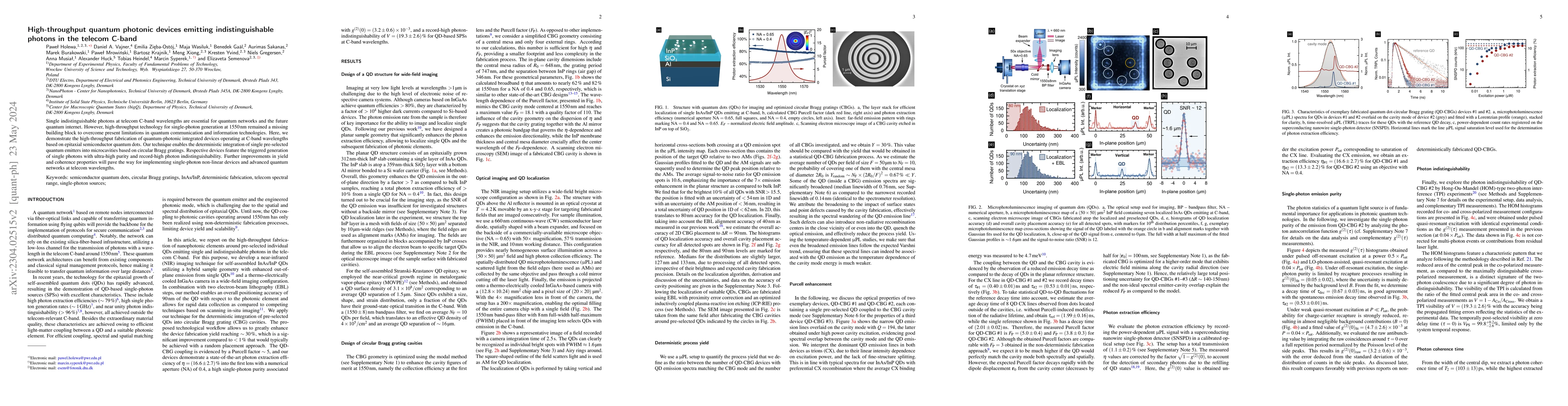
Single indistinguishable photons at telecom C-band wavelengths are essential for quantum networks and the future quantum internet. However, high-throughput technology for single-photon generation at...
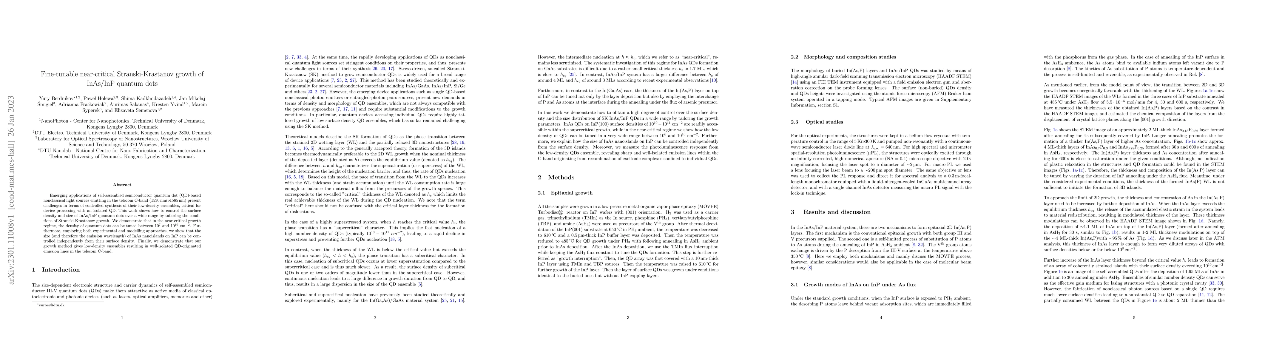
Emerging applications of self-assembled semiconductor quantum dot (QD)-based nonclassical light sources emitting in the telecom C-band (1530 to 1565 nm) present challenges in terms of controlled syn...
In its 60 years of existence, the field of nonlinear optics has gained momentum especially over the past two decades thanks to major breakthroughs in material science and technology. In this article...
The explorations of physical degrees of freedom with infinite dimensionalities, such as orbital angular momentum and frequency of light, have profoundly reshaped the landscape of modern optics with ...
Light sources with ultra-low energy consumption and high performance are required to realize optical interconnects for on-chip communication. Photonic crystal (PhC) nanocavity lasers are one of the ...
Whereas the Si photonic platform is highly attractive for scalable optical quantum information processing, it lacks practical solutions for efficient photon generation. Self-assembled semiconductor ...
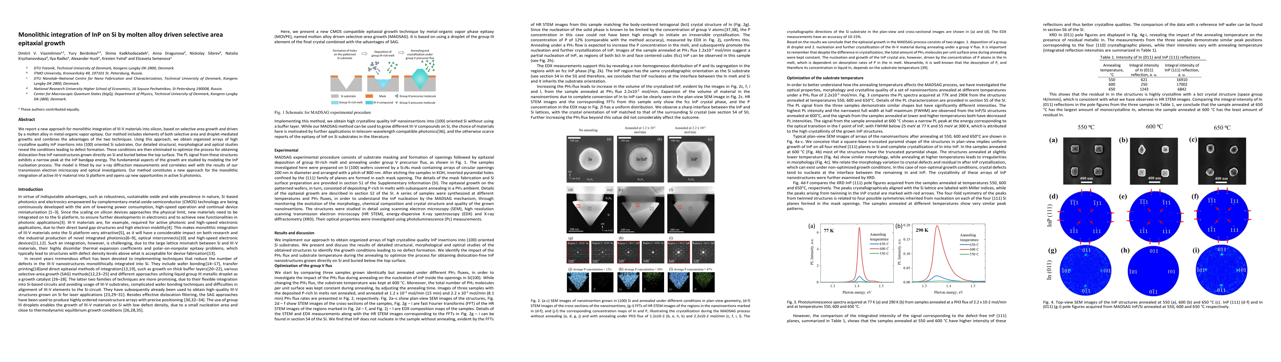
We report a new approach for monolithic integration of III-V materials into silicon, based on selective area growth and driven by a molten alloy in metal-organic vapor epitaxy. Our method includes e...
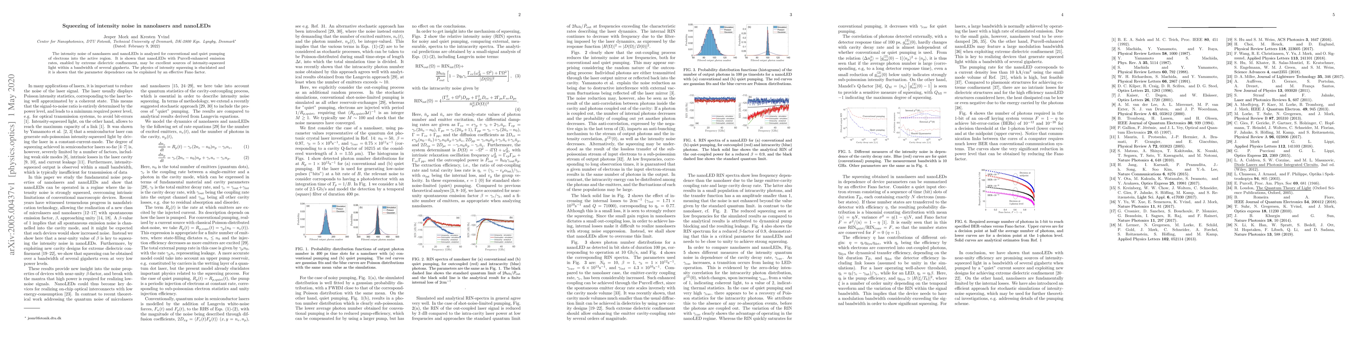
The intensity noise of nanolasers and nanoLEDs is analyzed for conventional and quiet pumping of electrons into the active region. It is shown that nanoLEDs with Purcell-enhanced emission rates, ena...
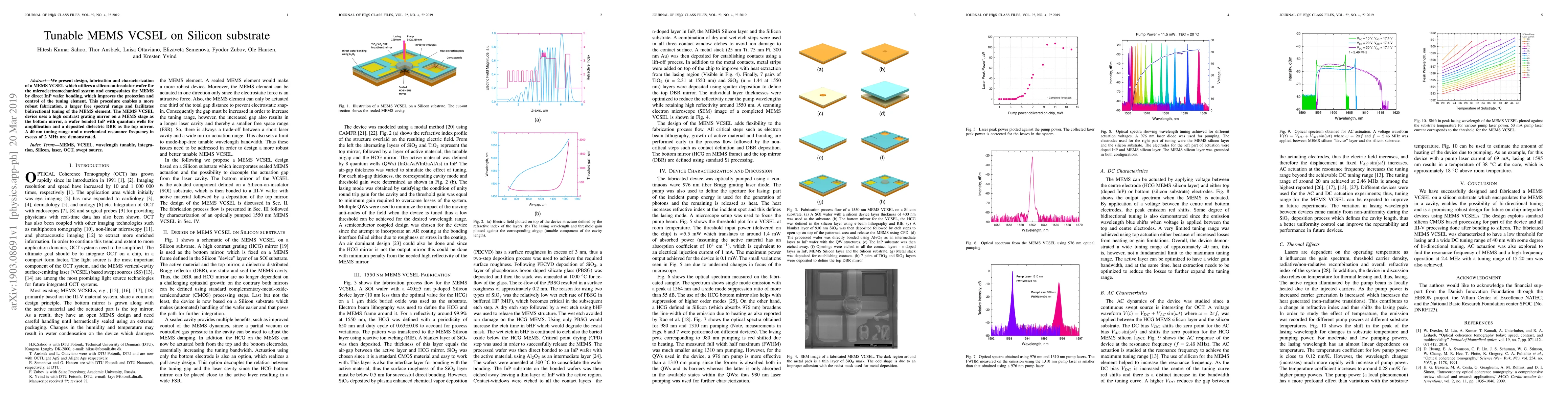
We present design, fabrication and characterization of a MEMS VCSEL which utilizes a silicon-on-insulator wafer for the microelectromechanical system and encapsulates the MEMS by direct InP wafer bo...
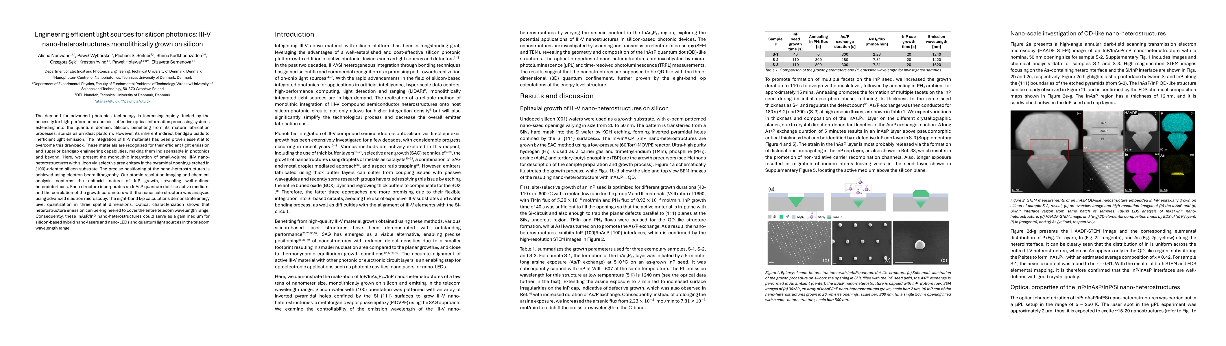
The demand for advanced photonics technology is increasing rapidly, fueled by the necessity for high-performance and cost-effective optical information processing systems extending into the quantum do...
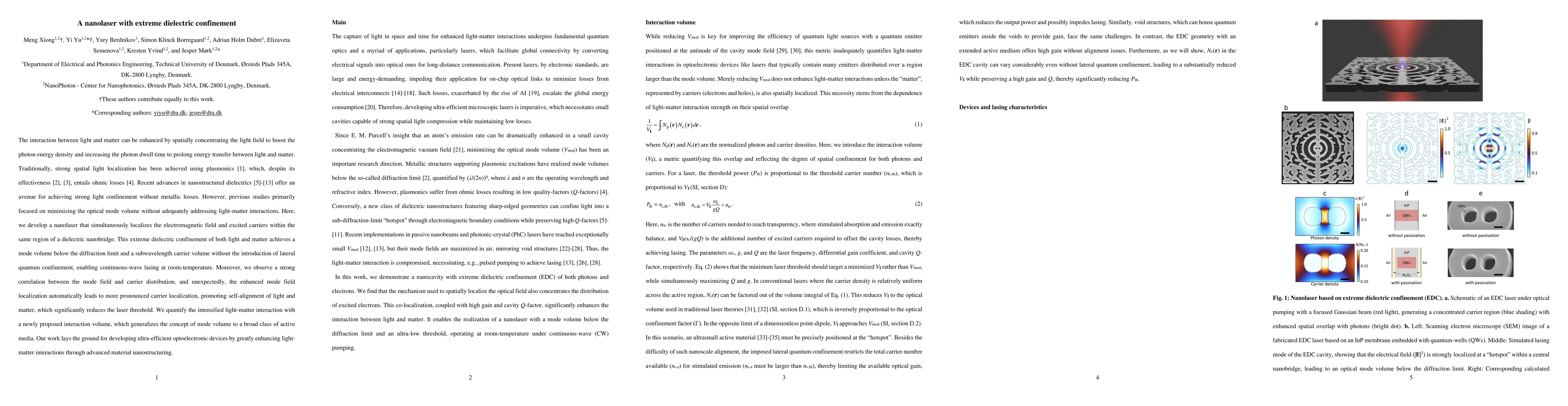
The interaction between light and matter can be enhanced by spatially concentrating the light field to boost the photon energy density and increasing the photon dwell time to prolong energy transfer b...
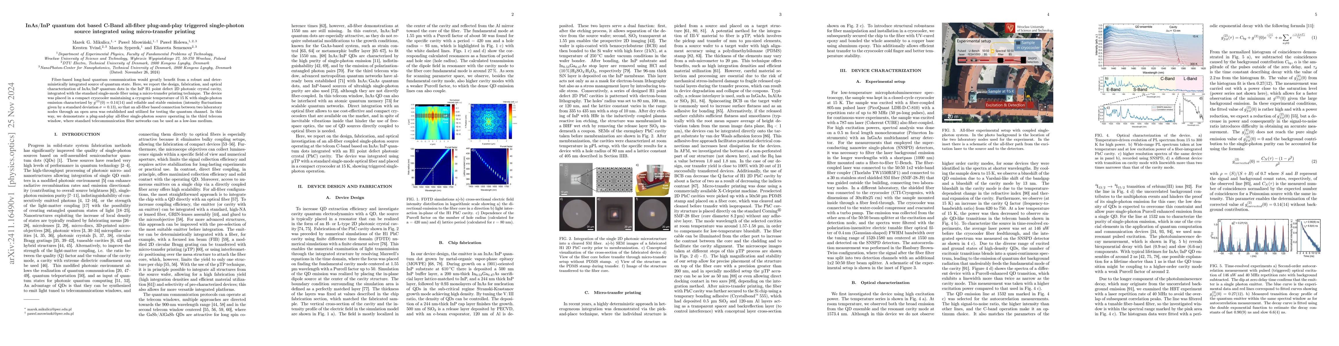
Fiber-based long-haul quantum communication would greatly benefit from a robust and deterministically integrated source of quantum state. Here, we report the design, fabrication, and optical character...
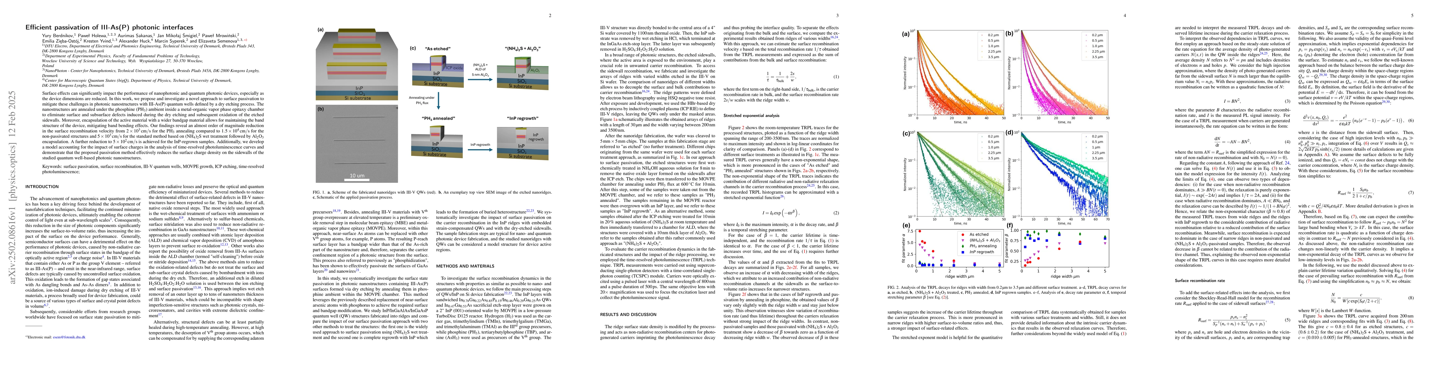
Surface effects can significantly impact the performance of nanophotonic and quantum photonic devices, especially as the device dimensions are reduced. In this work, we propose and investigate a novel...
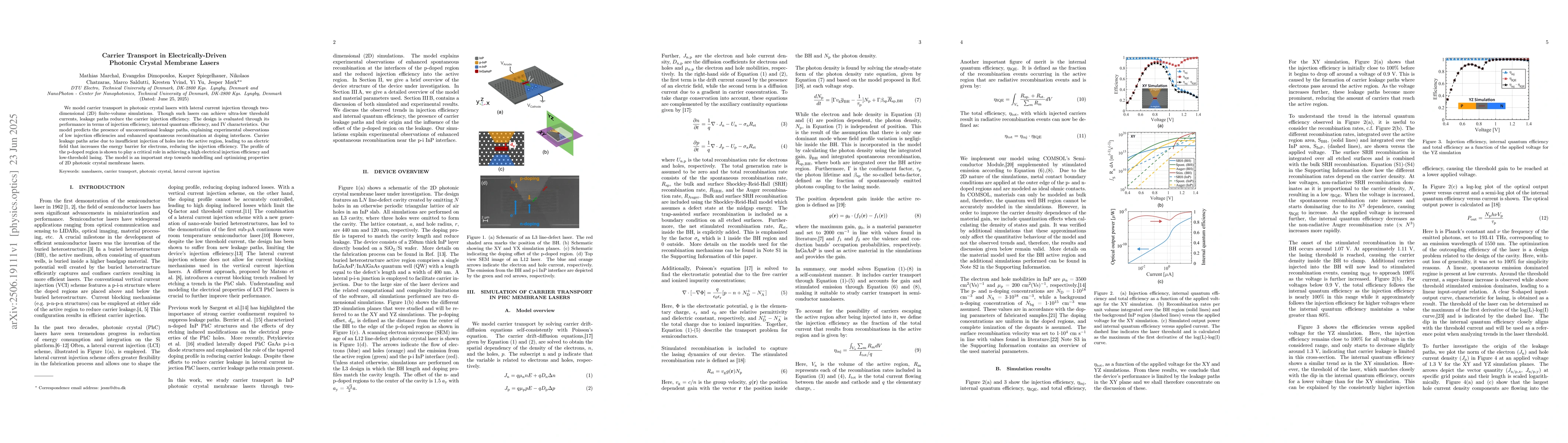
We model carrier transport in photonic crystal lasers with lateral current injection through two-dimensional (2D) finite-volume simulations. Though such lasers can achieve ultra-low threshold currents...
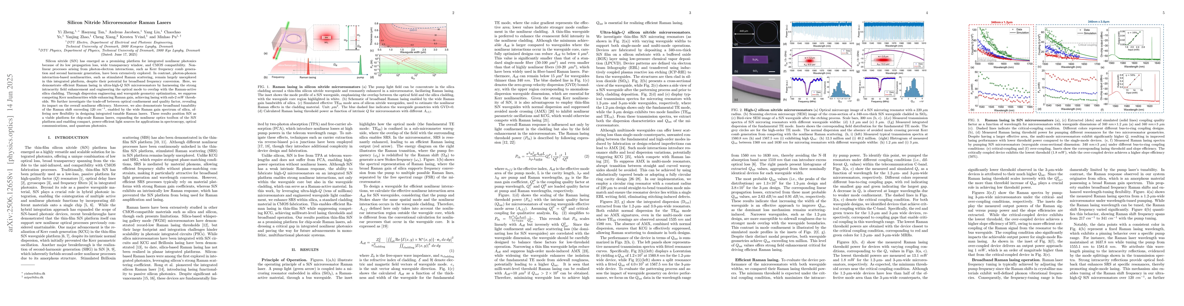
Silicon nitride (SiN) has emerged as a promising platform for integrated nonlinear photonics because of its low propagation loss, wide transparency window, and CMOS compatibility. Nonlinear processes ...
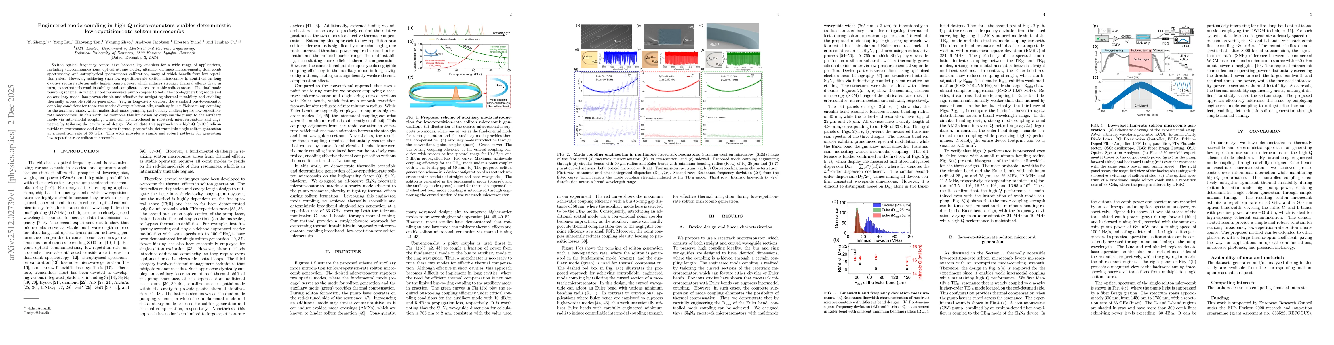
Soliton optical frequency combs have become key enablers for a wide range of applications, including telecommunications, optical atomic clocks, ultrafast distance measurements, dual-comb spectroscopy,...
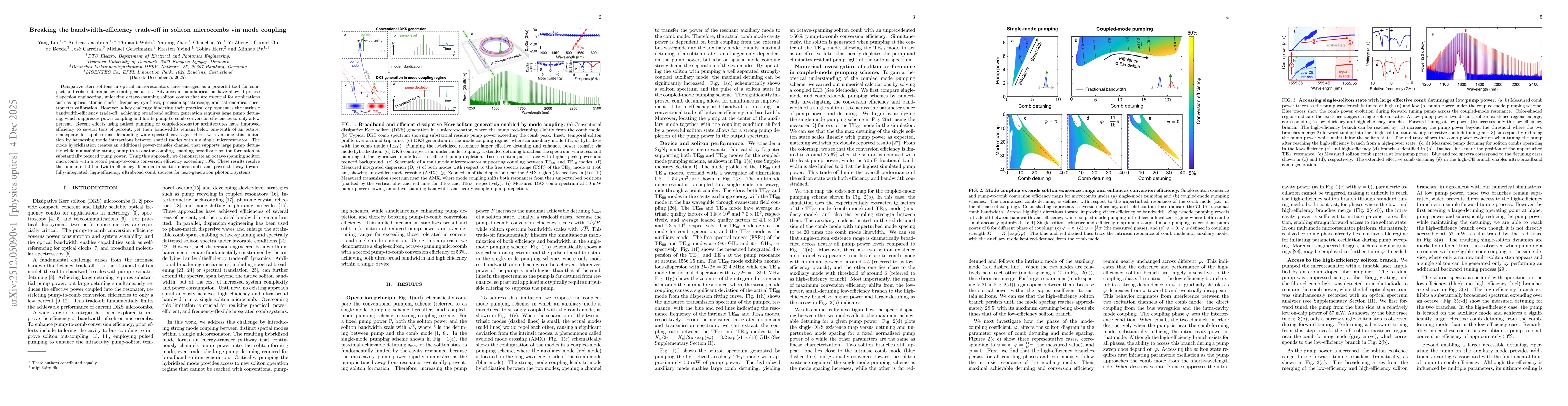
Dissipative Kerr solitons in optical microresonators have emerged as a powerful tool for compact and coherent frequency comb generation. Advances in nanofabrication have allowed precise dispersion eng...
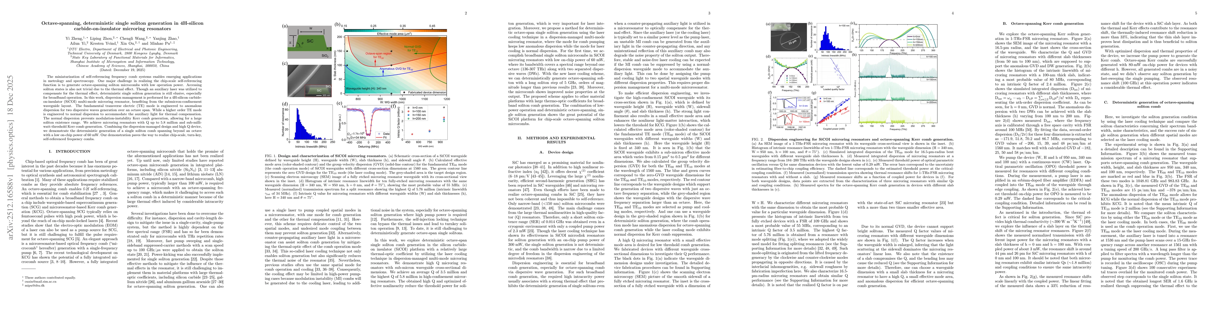
The miniaturization of self-referencing frequency comb systems enables emerging applications in metrology and spectroscopy. One major challenge in realizing the chip-scale self-referencing function is...
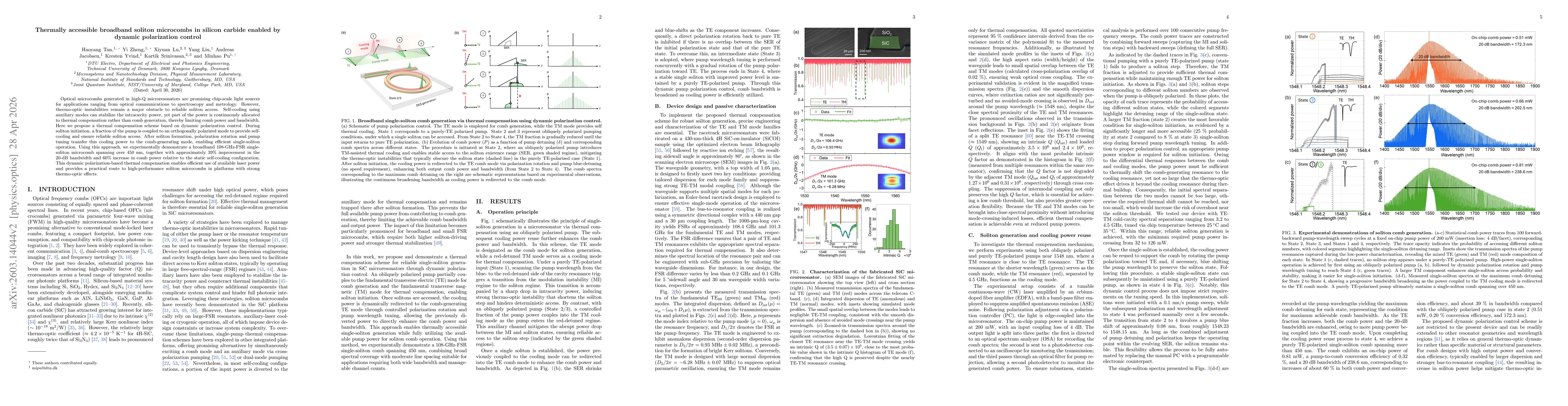
Optical microcombs generated in high-Q microresonators are promising chip-scale light sources for applications ranging from optical communications to spectroscopy and metrology. However, thermo-optic ...
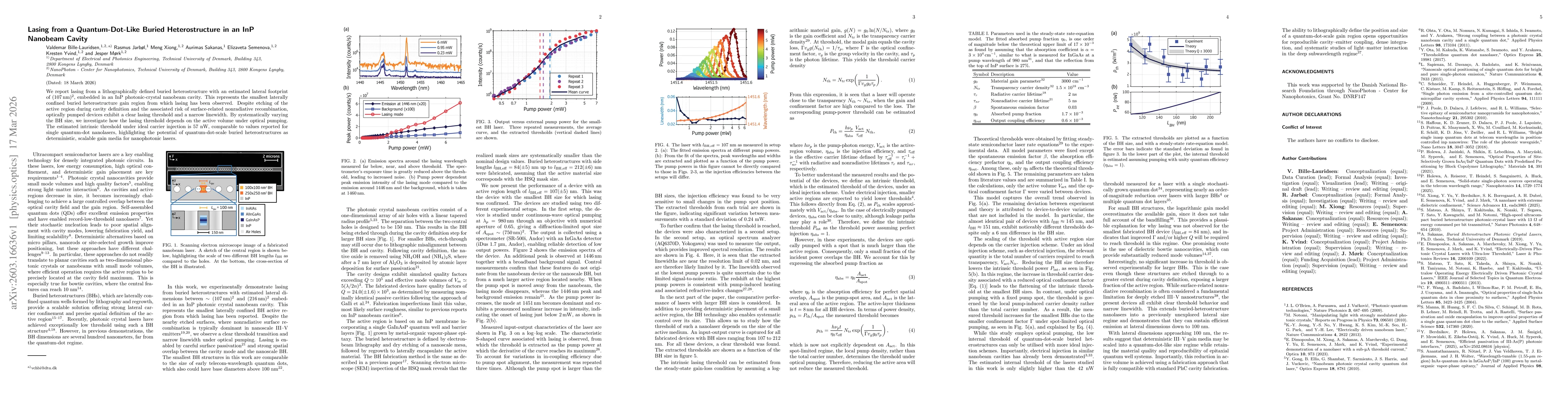
We report lasing from a lithographically defined buried heterostructure with an estimated lateral footprint of (107 nm)^2, embedded in an InP photonic-crystal nanobeam cavity. This represents the smal...
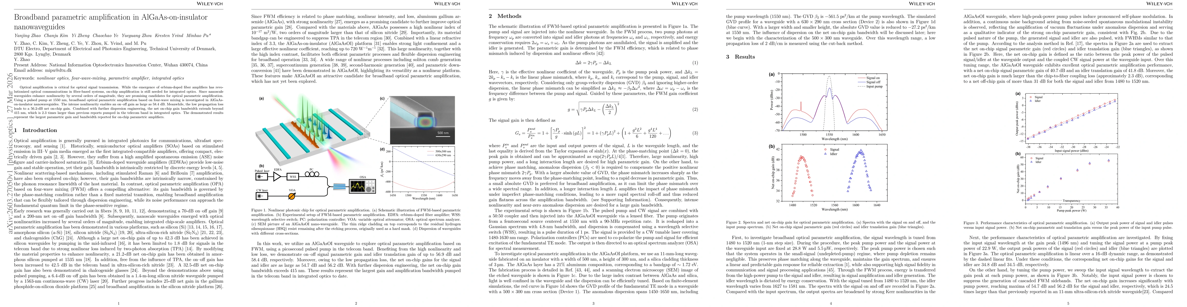
Optical amplification is critical for optical signal transmission. While the emergence of erbium-doped fiber amplifiers has revolutionized optical communications in fiber-based systems, on-chip amplif...
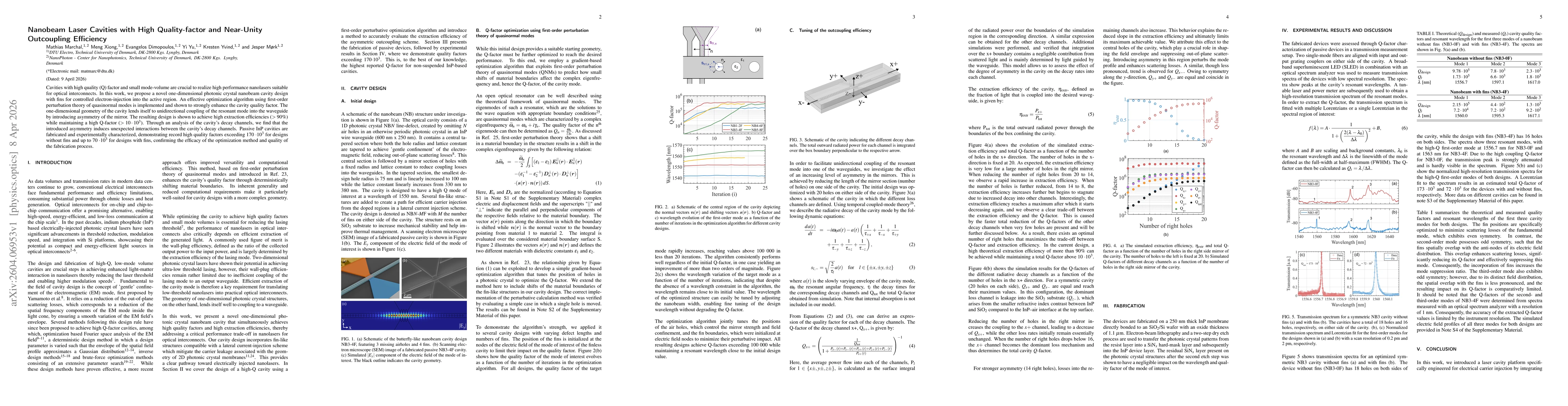
Cavities with high quality (Q) factor and small mode-volume are crucial to realize high performance nanolasers suitable for optical interconnects. In this work, we propose a novel one-dimensional phot...
Dissipative Kerr soliton microcombs enable compact and scalable frequency comb sources for precision metrology, spectroscopy, communications and coherent LiDAR, where broad and reliable frequency tuni...