Publication
Metrics
AI Quick Summary
This research demonstrates the integration of self-assembled InAs/InP quantum dots into silicon-on-insulator (SOI) chips using direct bonding, enabling efficient coupling of single photons for quantum photonic applications. The method shows 5.1% directional on-chip photon coupling efficiency, crucial for scalable quantum photonic systems.
Paper Preview
Abstract
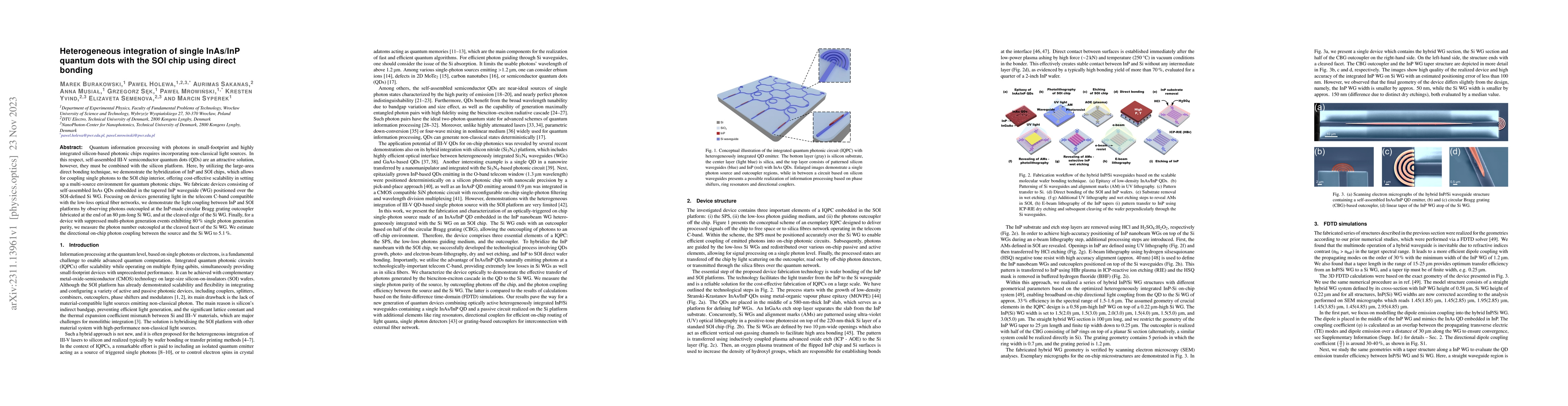
Quantum information processing with photons in small-footprint and highly integrated silicon-based photonic chips requires incorporating non-classical light sources. In this respect, self-assembled III-V semiconductor quantum dots (QDs) are an attractive solution, however, they must be combined with the silicon platform. Here, by utilizing the large-area direct bonding technique, we demonstrate the hybridization of InP and SOI chips, which allows for coupling single photons to the SOI chip interior, offering cost-effective scalability in setting up a multi-source environment for quantum photonic chips. We fabricate devices consisting of self-assembled InAs QDs embedded in the tapered InP waveguide (WG) positioned over the SOI-defined Si WG. Focusing on devices generating light in the telecom C-band compatible with the low-loss optical fiber networks, we demonstrate the light coupling between InP and SOI platforms by observing photons outcoupled at the InP-made circular Bragg grating outcoupler fabricated at the end of an 80 $\mu$m-long Si WG, and at the cleaved edge of the Si WG. Finally, for a device with suppressed multi-photon generation events exhibiting 80% single photon generation purity, we measure the photon number outcoupled at the cleaved facet of the Si WG. We estimate the directional on-chip photon coupling between the source and the Si WG to 5.1%.
AI Key Findings
Get AI-generated insights about this paper's methodology, results, significance, and more — seven facets brought into focus.
Impact
Paper Details
Authors
PDF Preview
Key Terms
Citation Network
Current paper (gray), citations (green), references (blue)
Display is limited for performance on very large graphs.
Discussion 0