Publication
Metrics
AI Quick Summary
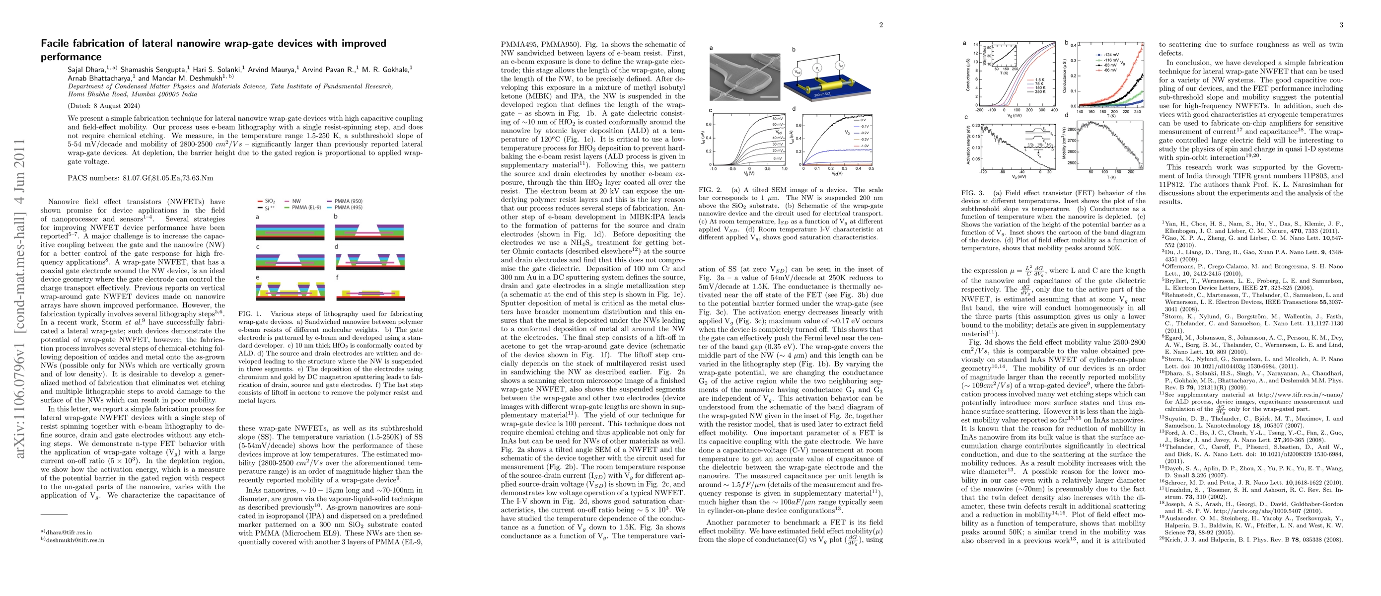
This paper describes a straightforward fabrication method for lateral nanowire wrap-gate devices that achieves high capacitive coupling and field-effect mobility without chemical etching. The technique shows improved performance with subthreshold slopes of 5-54 mV/decade and mobility ranging from 2800 to 2500 $cm^2/Vs$.
Paper Preview
Abstract
We present a simple fabrication technique for lateral nanowire wrap-gate devices with high capacitive coupling and field-effect mobility. Our process uses e-beam lithography with a single resist-spinning step, and does not require chemical etching. We measure, in the temperature range 1.5-250 K, a subthreshold slope of 5-54 mV/decade and mobility of 2800-2500 $cm^2/Vs$ -- significantly larger than previously reported lateral wrap-gate devices. At depletion, the barrier height due to the gated region is proportional to applied wrap-gate voltage.
AI Key Findings
Get AI-generated insights about this paper's methodology, results, significance, and more — seven facets brought into focus.
Impact
Paper Details
PDF Preview
Key Terms
Citation Network
Current paper (gray), citations (green), references (blue)
Display is limited for performance on very large graphs.
Discussion 0