Quick Summary:

This paper describes a fabrication method for horizontal wrap-gate InAs nanowire transistors with up to four independently controllable segments, highlighting the scalability advantage over vertical designs. The technique exhibits negligible cross-talk between segments and suggests potential for advanced 3D nanowire network architectures.

Summary

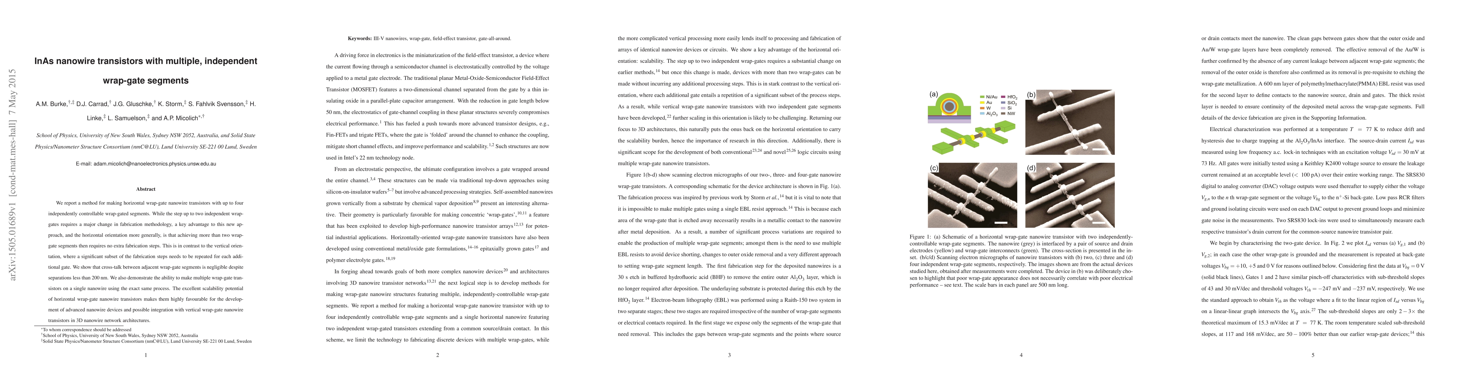
We report a method for making horizontal wrap-gate nanowire transistors with up to four independently controllable wrap-gated segments. While the step up to two independent wrap-gates requires a major change in fabrication methodology, a key advantage to this new approach, and the horizontal orientation more generally, is that achieving more than two wrap-gate segments then requires no extra fabrication steps. This is in contrast to the vertical orientation, where a significant subset of the fabrication steps needs to be repeated for each additional gate. We show that cross-talk between adjacent wrap-gate segments is negligible despite separations less than 200 nm. We also demonstrate the ability to make multiple wrap-gate transistors on a single nanowire using the exact same process. The excellent scalability potential of horizontal wrap-gate nanowire transistors makes them highly favourable for the development of advanced nanowire devices and possible integration with vertical wrap-gate nanowire transistors in 3D nanowire network architectures.

AI Key Findings

Get AI-generated insights about this paper's methodology, results, and significance.

Paper Details

PDF Preview

Download PDF

Key Terms

gate (0.386)
nanowire (0.381)
gate (0.343)
horizontal (0.300)
segments (0.292)
segments (0.274)
fabrication (0.271)
vertical (0.217)
vertical (0.213)
steps (0.199)
orientation (0.195)
orientation (0.192)
steps (0.176)
requires (0.163)
requires (0.155)
separations (0.143)
gates (0.142)
controllable (0.137)
adjacent (0.133)
repeated (0.132)
Title Authors Year Actions
Reversible Carrier Modulation in InP Nanolasers by Ionic Liquid Gating with Low Energy Consumption.
Chia-Hung Wu, Chi-Wen Chen, Hung‐Jung Shen, Hsiang-Yu Chuang, Hark Hoe Tan, C. Jagadish, Tien-Chang Lu, Satoshi Ishii, Kuo-Ping Chen
2024
View Paper
Continuous Microwave Photon Counting by Semiconductor-Superconductor Hybrids.
S. Haldar, David Barker, H. Havir, A. Ranni, Sebastian Lehmann, Kimberly A. Dick, V. F. Maisi
2024
View Paper
Simulation of a Vertical Ballistic Quantum-Barrier Field-Effect Transistor Based on an Undoped AlxGa1–xAs Quantum Nanowire
D. V. Pozdnyakov, A. Borzdov, V. Borzdov
2023
View Paper
Calculation of Electrophysical Characteristics of Semiconductor Quantum Wire Device Structures with One-Dimensional Electron Gas
D. V. Pozdnyakov, A. Borzdov, V. Borzdov
2023
View Paper
Simulation of vertical ballistic quantum-barrier field-effect transistor based on undoped AlxGa1–xAs quantum nanowire
D. V. Pozdnyakov, A. Borzdov, V. Borzdov
2023
View Paper
In‐Plane Integrating Unidirectional 1D CsPbBr3 Waveguide Arrays with Heterogeneous Semiconductor Wires for Photonic Integrated Circuits
Sha Jiang, Xing Xu, Chao Fan, Long Chen, Lei Shen, Qi Deng, Xue Xia, Q. Zhang
2023
View Paper
Buried graphene heterostructures for electrostatic doping of low-dimensional materials
A. Gumprich, J. Liedtke, S. Beck, I. Chirca, T. Potočnik, J. Alexander-Webber, S. Hofmann, S. Tappertzhofen
2023
View Paper
Large-Area Homogeneous Corrosion Process for Electrochemical Nanoimprint Lithography on GaAs Wafer by Modulating Contact Pressure
Qinghui Meng, Lianhuan Han, Hantao Xu, Xiaoting Lin, J. Zhang, Yunfeng Peng, Jianlin Su, D. Zhan
2022
View Paper
Te-doped selective-area grown InAs nanowires for superconducting hybrid devices
P. Perla, Anton Faustmann, Sebastian Koelling, P. Zellekens, R. Deacon, H. Aruni Fonseka, J. Kölzer, Yuki Sato, A. Sánchez, O. Moutanabbir, K. Ishibashi, D. Grützmacher, M. Lepsa, T. Schäpers
2021
View Paper
Dispersive one-dimensional Majorana modes with emergent supersymmetry in one-dimensional proximitized superconductors via spatially modulated potentials and magnetic fields
P. Marra, D. Inotani, M. Nitta
2021
View Paper
Synthesis and thermal reaction of stainless steel nanowires.
G. Csiszár, M. Schellenberger, G. Schmitz
2019
View Paper
Quantum Transport in GaAs/InSb core-shell nanowires
P. Zellekens, N. Demarina, J. Janßen, T. Rieger, M. Lepsa, P. Perla, G. Panaitov, H. Lüth, D. Grützmacher, T. Schäpers
2019
View Paper
Anodic Imprint Lithography: Direct Imprinting of Single Crystalline GaAs with Anodic Stamp.
Kyunghwan Kim, Bugeun Ki, Keorock Choi, Jungwoo Oh
2019
View Paper
Absolute Seebeck coefficient of thin platinum films
M. Kockert, R. Mitdank, A. Zykov, S. Kowarik, S. F. Fischer
2019
View Paper
Transition to the quantum hall regime in InAs nanowire cross-junctions
J. Gooth, M. Borg, H. Schmid, N. Bologna, M. Rossell, S. Wirths, K. Moselund, K. Nielsch, H. Riel
2019
View Paper
Coupled Ion‐Gel Channel‐Width Gating and Piezotronic Interface Gating in ZnO Nanowire Devices
Xixi Yang, Guofeng Hu, Guoyun Gao, Xuanyu Chen, Junlu Sun, Bensong Wan, Qian Zhang, Shanshan Qin, Wenliang Zhang, Caofeng Pan, Qijun Sun, Zhong Lin Wang
2019
View Paper
Achieving short high-quality gate-all-around structures for horizontal nanowire field-effect transistors
J. G. Gluschke, J. Seidl, Adam Burke, R. Lyttleton, D. Carrad, A. R. Ullah, S. Fahlvik, S. Lehmann, Heiner Linke, A. Micolich
2018
View Paper
p-GaAs Nanowire Metal-Semiconductor Field-Effect Transistors with Near-Thermal Limit Gating.
A. R. Ullah, F. Meyer, J. G. Gluschke, S. Naureen, P. Caroff, P. Caroff, P. Krogstrup, J. Nygård, A. Micolich
2018
View Paper
Charge carrier-selective contacts for nanowire solar cells
Sebastian Z. Oener, A. Cavalli, Hongyu Sun, J. Haverkort, E. Bakkers, E. Garnett
2018
View Paper
Using Ultrathin Parylene Films as an Organic Gate Insulator in Nanowire Field-Effect Transistors.
J. G. Gluschke, J. Seidl, R. Lyttleton, D. Carrad, D. Carrad, J. Cochrane, S. Lehmann, L. Samuelson, A. Micolich
2018
View Paper
Controllable directive radiation from dipole emitter coupled to dielectric nanowire antenna with substrate-mediated tunability
M. M. Salary, A. Forouzmand, H. Mosallaei
2018
View Paper
Advanced platform for the in-plane ZT measurement of thin films.
V. Linseis, F. Völklein, H. Reith, K. Nielsch, P. Woias
2018
View Paper
Near-thermal limit gating in heavily-doped III-V semiconductor nanowires using polymer electrolytes.
A. R. Ullah, D. J. Carrad, P. Krogstrup, J. Nygaard, A. Micolich
2017
View Paper
Buried multi-gate InAs-nanowire FETs
T. Grap, Felix Riederer, Charu Gupta, J. Knoch
2017
View Paper
Electrically Tunable Metamaterials Based on Multimaterial Nanowires Incorporating Transparent Conductive Oxides
M. M. Salary, H. Mosallaei
2017
View Paper
Ultrathin strain-gated field effect transistor based on In-doped ZnO nanobelts
Zheng Zhang, Junli Du, Bing-Jing Li, Shuhao Zhang, Mengyu Hong, Xiaomei Zhang, Qingliang Liao, Yue Zhang
2017
View Paper
Horizontal InAs nanowire transistors grown on patterned silicon-on-insulator substrate
Wang Zhang, Weihua Han, Xiaosong Zhao, Qi-Feng Lv, X. Ji, Tao Yang, Fuhua Yang
2017
View Paper
Quantum Transport and Sub-Band Structure of Modulation-Doped GaAs/AlAs Core-Superlattice Nanowires.
Dominik M Irber, J. Seidl, D. J. Carrad, J. Becker, N. Jeon, B. Loitsch, Julia Winnerl, S. Matich, M. Döblinger, Yang Tang, S. Morkötter, G. Abstreiter, J. Finley, M. Grayson, L. Lauhon, G. Koblmüller
2017
View Paper
Catalyst shape engineering for anisotropic cross-sectioned nanowire growth
Y. Calahorra, A. Kelrich, S. Cohen, D. Ritter
2017
View Paper
Piezopotential-Programmed Multilevel Nonvolatile Memory As Triggered by Mechanical Stimuli.
Qijun Sun, D. Ho, Yongsuk Choi, Caofeng Pan, Do Hwan Kim, Zhong Lin Wang, J. Cho
2016
View Paper
Controllable Formation of Zinc Oxide Micro‐ and Nanostructures via DUV Direct Patterning
C. Yeh, H. Liu, M. Chuang, Joseph Denzer, D. Berling, H. Zan, O. Soppera
2016
View Paper
Platform for in-plane ZT measurement and Hall coefficient determination of thin films in a temperature range from 120 K up to 450 K
V. Linseis, F. Völklein, H. Reith, P. Woias, K. Nielsch
2016
View Paper
Development of Nanowire Patterning Process Using Microcontact Printing
Sungjin Jo
2016
View Paper
Electronic Properties of Complex Self‐Assembled InAs Nanowire Networks
S. Heedt, D. Vakulov, T. Rieger, Daniel Rosenbach, S. Trellenkamp, D. Grützmacher, M. Lepsa, T. Schäpers
2016
View Paper
In situ fabrication and investigation of nanostructures and nanodevices with a microscope.
Qi Zhang, Huiqiao Li, Lin Gan, Ying Ma, D. Golberg, T. Zhai
2016
View Paper
Microcantilever Printed CuO Single Nanowire Field-Effect Transistors for Sensing Applications
S. Raveesh, V. Yadav, R. Paily
2023
View Paper
Absolute Seebeck coefficient of thin platinum films Absolute Seebeck coefficient of thin platinum films
M. Kockert, R. Mitdank, A. Zykov, S. Kowarik, S. F. Fischer
2019
View Paper
Electronic applications of oxide nanostructures
D. Nunes, A. Pimentel, Lídia Santos, P. Barquinha, L. Pereira, E. Fortunato, R. Martins
2019
View Paper
p ‐ GaAs Nanowire Metal − Semiconductor Field-E ff ect Transistors with Near-Thermal Limit Gating
A. R. Ullah, F. Meyer, J. G. Gluschke, S. Naureen, P. Caro, P. Krogstrup, J. Nygård, A. Micolich
2018
View Paper
Using ultra-thin parylene films as an organic gate insulator in nanowire field-effect transistors
J. G. Gluschke, J. Seidl, R. Lyttleton, D. J. Carrad, J. Cochrane, S., Lehmann, L. Samuelson, A. Micolich
2018
View Paper
Analysis of Ge-Si Heterojunction Nanowire Tunnel FET: Impact of Tunneling Window of Band-to-Band Tunneling Model
E. D. Kurniawan, Shang-Yi Yang, V. Thirunavukkarasu, Yung-Chun Wu
2017
View Paper

Comments (0)

This website uses cookies to ensure you get the best experience. Learn more