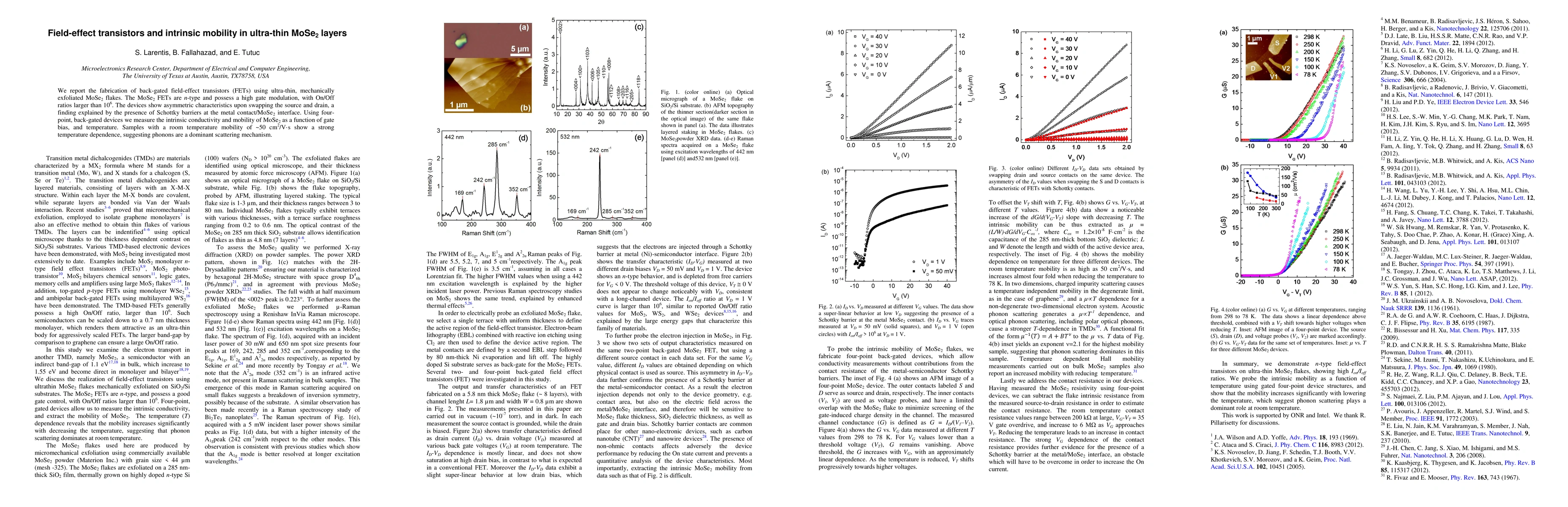
Publication
Metrics
AI Quick Summary
This paper reports the fabrication of n-type back-gated field-effect transistors using ultra-thin MoSe2 flakes, showing high gate modulation and On/Off ratios exceeding 106. The study reveals intrinsic conductivity and mobility of MoSe2, with room temperature mobility around 50 cm2/V.s, and identifies phonon scattering as a dominant mechanism.
Paper Preview
Abstract
We report the fabrication of back-gated field-effect transistors (FETs) using ultra-thin, mechanically exfoliated MoSe2 flakes. The MoSe2 FETs are n-type and possess a high gate modulation, with On/Off ratios larger than 106. The devices show asymmetric characteristics upon swapping the source and drain, a finding explained by the presence of Schottky barriers at the metal contact/MoSe2 interface. Using four-point, back-gated devices we measure the intrinsic conductivity and mobility of MoSe2 as a function of gate bias, and temperature. Samples with a room temperature mobility of ~50 cm2/V.s show a strong temperature dependence, suggesting phonons are a dominant scattering mechanism.
AI Key Findings
Get AI-generated insights about this paper's methodology, results, significance, and more — seven facets brought into focus.
Impact
Paper Details
PDF Preview
Key Terms
Citation Network
Current paper (gray), citations (green), references (blue)
Display is limited for performance on very large graphs.
Discussion 0