Publication
Metrics
AI Quick Summary
This paper evaluates CdTe as a tunnel barrier at the $\alpha$-Sn/InSb interface using density functional theory with Hubbard U corrections and machine-learning techniques. It finds that 16 atomic layers of CdTe can effectively shield InSb from metal-induced gap states, suggesting its potential use in mediating coupling in topological quantum computing devices.
Paper Preview
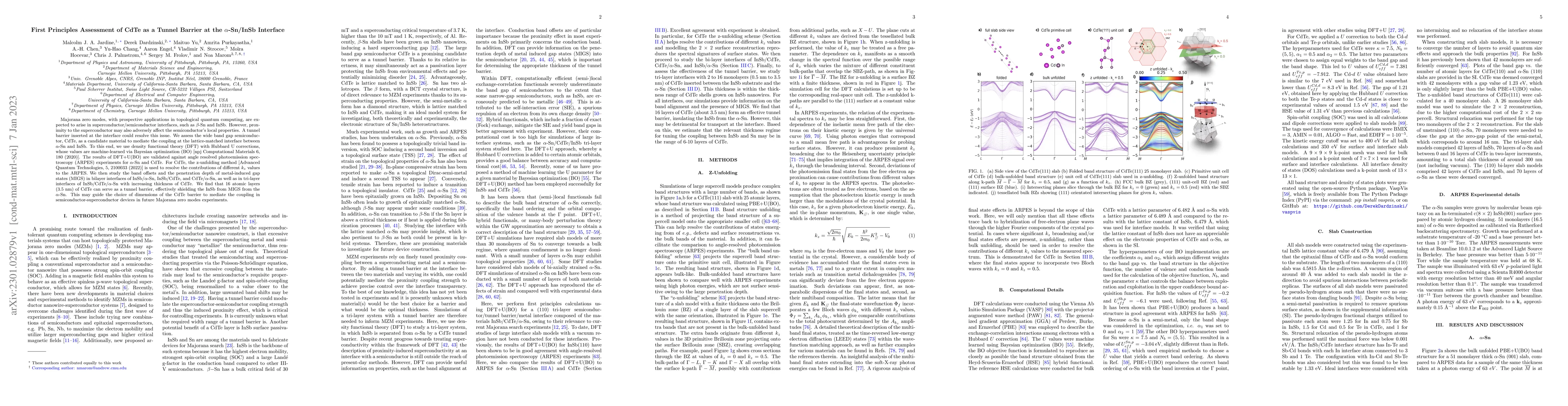
Abstract
Majorana zero modes, with prospective applications in topological quantum computing, are expected to arise in superconductor/semiconductor interfaces, such as $\beta$-Sn and InSb. However, proximity to the superconductor may also adversely affect the semiconductor's local properties. A tunnel barrier inserted at the interface could resolve this issue. We assess the wide band gap semiconductor, CdTe, as a candidate material to mediate the coupling at the lattice-matched interface between $\alpha$-Sn and InSb. To this end, we use density functional theory (DFT) with Hubbard U corrections, whose values are machine-learned via Bayesian optimization (BO) [npj Computational Materials 6, 180 (2020)]. The results of DFT+U(BO) are validated against angle resolved photoemission spectroscopy (ARPES) experiments for $\alpha$-Sn and CdTe. For CdTe, the z-unfolding method [Advanced Quantum Technologies, 5, 2100033 (2022)] is used to resolve the contributions of different $k_z$ values to the ARPES. We then study the band offsets and the penetration depth of metal-induced gap states (MIGS) in bilayer interfaces of InSb/$\alpha$-Sn, InSb/CdTe, and CdTe/$\alpha$-Sn, as well as in tri-layer interfaces of InSb/CdTe/$\alpha$-Sn with increasing thickness of CdTe. We find that 16 atomic layers (3.5 nm) of CdTe can serve as a tunnel barrier, effectively shielding the InSb from MIGS from the $\alpha$-Sn. This may guide the choice of dimensions of the CdTe barrier to mediate the coupling in semiconductor-superconductor devices in future Majorana zero modes experiments.
AI Key Findings
Get AI-generated insights about this paper's methodology, results, significance, and more — seven facets brought into focus.
Impact
Paper Details
Authors
PDF Preview
Key Terms
Citation Network
Current paper (gray), citations (green), references (blue)
Display is limited for performance on very large graphs.
Discussion 0