The study utilized Monte Carlo simulations and experimental micrographs acquired under various conditions to analyze imaging contrast inversions in a Zr-Nb alloy with nano-precipitates using the ARGUS system in a SEM.
Publication
Metrics
AI Quick Summary
This study investigates imaging contrast inversions in a Zr-Nb alloy using forescattered electron imaging in a SEM, proposing conditions that enhance atomic number or diffraction contrast. The ARGUSTM system's results are compared with those from TEM and STEM, demonstrating its effectiveness in nanoscale microstructure analysis.
Quick Answers
What is "Forescattered electron imaging of nanoparticles in a scanning electron microscopy" about?
This study investigates imaging contrast inversions in a Zr-Nb alloy using forescattered electron imaging in a SEM, proposing conditions that enhance atomic number or diffraction contrast. The ARGUSTM system's results are compared with those from TEM and STEM, demonstrating its effectiveness in nanoscale microstructure analysis.
What methodology did the authors use?
The study utilized Monte Carlo simulations and experimental micrographs acquired under various conditions to analyze imaging contrast inversions in a Zr-Nb alloy with nano-precipitates using the ARGUS system in a SEM. More in Methodology →
What are the key results?
Imaging conditions enhancing atomic number or diffraction contrast were proposed. — The ARGUS system demonstrated capability to investigate microstructures in nano-scale materials, as evidenced by comparison with results from standard TEM and STEM imaging. More in Key Results →
Why is this work significant?
This research indicates that imaging thin foils in transmission with forescattered electrons in an SEM is suitable for investigating the microstructure of engineering materials, including embedded small nanoparticles, without the need for expensive TEM or STEM instrumentation. More in Significance →
What are the main limitations?
The study was limited to a specific Zr-Nb alloy model material. — Experimental validation was conducted on a single material system. More in Limitations →
Abstract
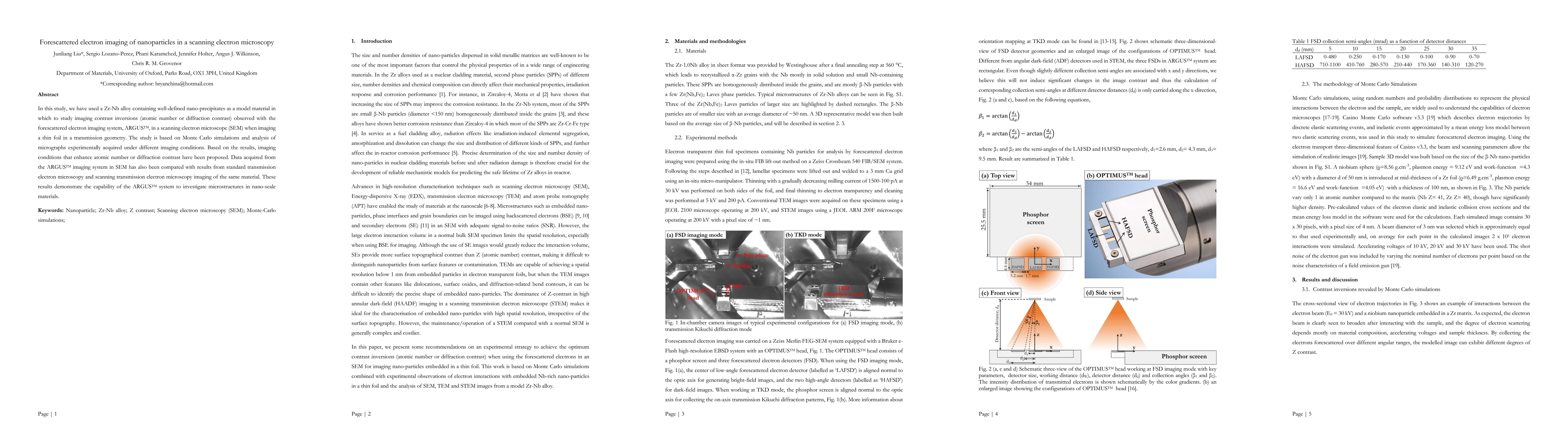
In this study, we have used a Zr-Nb alloy containing well-defined nano-precipitates as a model material in which to study imaging contrast inversions (atomic number or diffraction contrast) observed with the forescattered electron imaging system, ARGUSTM, in a scanning electron microscope (SEM) when imaging a thin foil in a transmission geometry. The study is based on Monte Carlo simulations and analysis of micrographs experimentally acquired under different imaging conditions. Based on the results, imaging conditions that enhance atomic number or diffraction contrast have been proposed. Data acquired from the ARGUSTM imaging system in SEM has also been compared with results from standard transmission electron microscopy and scanning transmission electron microscopy imaging of the same material. These results demonstrate the capability of the ARGUSTM system to investigate microstructures in nano-scale materials.
Key Findings, in focus
Seven facets of this paper, analysed and brought into focus by AI.
This research indicates that imaging thin foils in transmission with forescattered electrons in an SEM is suitable for investigating the microstructure of engineering materials, including embedded small nanoparticles, without the need for expensive TEM or STEM instrumentation.
- Imaging conditions enhancing atomic number or diffraction contrast were proposed.
- The ARGUS system demonstrated capability to investigate microstructures in nano-scale materials, as evidenced by comparison with results from standard TEM and STEM imaging.
- Contrast reversals were found to occur depending on collection angles and accelerating voltages.
- Critical detector distances for optimizing contrast conditions were determined using Monte Carlo simulations.
- Small features <1 nm, such as dislocations, can be reliably detected using FSD imaging.
This research indicates that imaging thin foils in transmission with forescattered electrons in an SEM is suitable for investigating the microstructure of engineering materials, including embedded small nanoparticles, without the need for expensive TEM or STEM instrumentation.
The development of Monte Carlo simulations to determine critical detector distances for optimizing contrast conditions in forescattered electron imaging, enabling users to select suitable imaging parameters for various materials.
The research presents a novel approach to studying microstructures in nano-scale materials using lower accelerating voltages (<10 kV) in an SEM, which is less damaging to electron beam-sensitive materials compared to traditional TEM and STEM techniques.
- The study was limited to a specific Zr-Nb alloy model material.
- Experimental validation was conducted on a single material system.
- Apply the findings to a wider range of materials systems.
- Investigate the imaging of dynamic processes in materials using FSD imaging.
Impact
Paper Details
PDF Preview
Key Terms
Citation Network
Current paper (gray), citations (green), references (blue)
Display is limited for performance on very large graphs.
Discussion 0