Gate-controllable electronic trap detection in dielectrics
Publication
Metrics
Paper Preview
Abstract
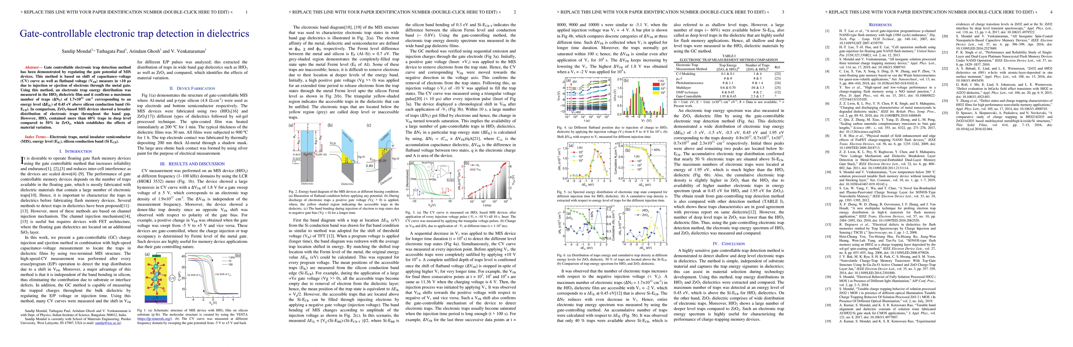
Gate controllable electronic trap detection method has been demonstrated by regulating the gate potential of MIS devices. This method is based on shift of capacitance voltage (CV) curve as well as flatband voltage (VFB) measure in less than 10 micro-seconds due to injection or ejection of electrons through the metal gate. Using this method, an electronic trap energy distribution was measured in the HfO2 dielectric film and it confirms a maximum number of traps (Delta_NT) of 1.7x1012 cm-2 corresponding to an energy level (Delta_EIL) of 0.45 eV above silicon conduction band (Si-ECB). In comparison, ZrO2-based MIS devices showed a broader distribution of electronic traps throughout the band gap. However, HfO2 contained more than 60% traps in deep level compared to 50% in ZrO2, which establishes the effects of material variation.
OpenAlex
- Citations in OpenAlex
- 2
- Publication year
- 2020
- Access status
- Open access
Source: OpenAlex · Snapshot
AI Key Findings
Get AI-generated insights about this paper's methodology, results, significance, and more — seven facets brought into focus.
Impact
Paper Details
Authors
PDF Preview
Key Terms
Citation Network
Current paper (gray), citations (green), references (blue)
Display is limited for performance on very large graphs.
Discussion 0