ArxivLens

Quick Summary:

This study investigates the gate-dependent Raman spectroscopy of CVD-grown graphene on hBN versus SiO$_2$ substrates, revealing that hBN produces fewer Raman peak fluctuations due to its atomically flat surface and lower charged impurities, compared to SiO$_2$. The G and 2D peak properties show distinct carrier density dependencies on the two substrates.

Journal Reference: J. Phys.: Condens. Matter 25 (2013) 505304
DOI: 10.1088/0953-8984/25/50/505304
arXiv Id: 1310.6663
Date Published: 2013-12-09
Date Updated: 2013-12-09

Key Terms (TF-IDF):

raman (0.312)
peak (0.307)
substrates (0.252)
carrier (0.227)
graphene (0.220)
_2 (0.207)
flat (0.191)
position (0.185)
area (0.182)
fluctuations (0.180)
charge (0.168)
density (0.161)
impurities (0.147)
charge density (0.146)
owing (0.143)
differs (0.142)
doping (0.142)
method used (0.141)
substrate (0.138)
fewer (0.135)
License: http://arxiv.org/licenses/nonexclusive-distrib/1.0/

Summary:

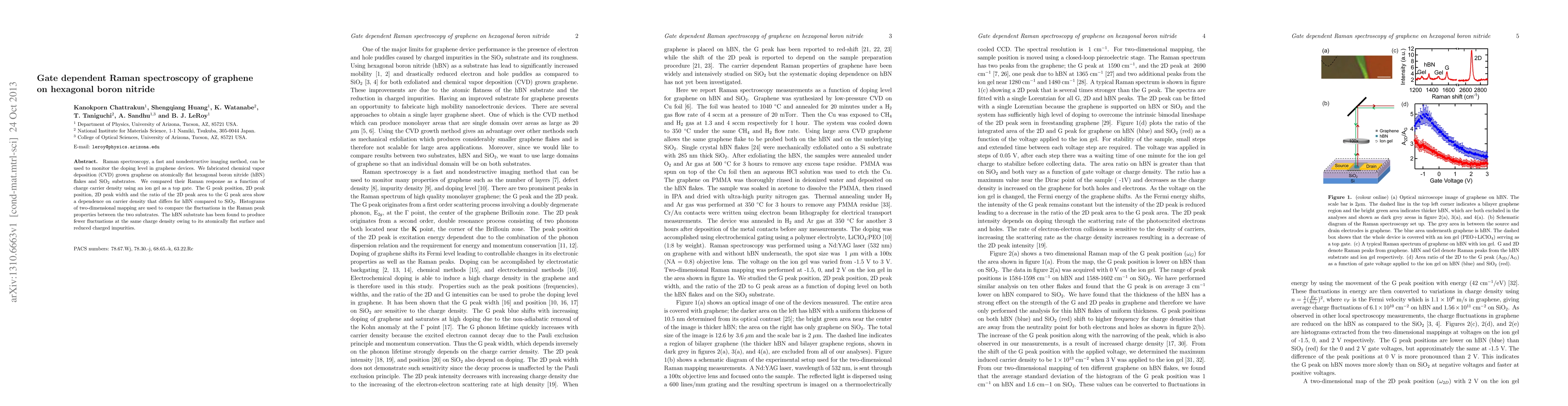
Raman spectroscopy, a fast and nondestructive imaging method, can be used to monitor the doping level in graphene devices. We fabricated chemical vapor deposition (CVD) grown graphene on atomically flat hexagonal boron nitride (hBN) flakes and SiO$_2$ substrates. We compared their Raman response as a function of charge carrier density using an ion gel as a top gate. The G peak position, 2D peak position, 2D peak width and the ratio of the 2D peak area to the G peak area show a dependence on carrier density that differs for hBN compared to SiO$_2$. Histograms of two-dimensional mapping are used to compare the fluctuations in the Raman peak properties between the two substrates. The hBN substrate has been found to produce fewer fluctuations at the same charge density owing to its atomically flat surface and reduced charged impurities.

Citation & Reference Network Visualization

This graph shows how this paper is connected to other research. The current paper is shown in dark gray, papers that cite it are in green, and papers it references are in blue. You can:

Current Paper
Papers citing this work (Citations)
Papers cited by this work (References)

• Hover over any node to see the paper title

• Click a node to view that paper's details

• Drag nodes to rearrange the graph

• Use the zoom controls (bottom right) to zoom in/out

Citations and References

Title Authors Year Actions
Charge carrier density dependent Raman spectra of graphene encapsulated in hexagonal boron nitride
J. Sonntag, Kenji Watanabe, T. Taniguchi, B. Beschoten, C. Stampfer
2023
View Paper
Raman spectroscopy as a probe for the electronic structure of graphene at electrified interfaces
Ruifeng Zhou, Hiro Minamimoto, Tomohiro Fukushima, K. Murakoshi
2022
View Paper
Design and fabrication of a large-range graphene/hexagonal boron nitride heterostructure based pressure sensor with poly(methyl methacrylate) substrate.
Guodong Zhang, Yulong Zhao, Jing Sun
2022
View Paper
Near-field probing of dielectric screening by hexagonal boron nitride in graphene integrated on silicon photonics
Binbin Wang, Sera Kim, T. Zhai, J. Seok, Heejun Yang, R. Salas-Montiel
2021
View Paper
Ultra-compact Spatial Terahertz Switch Based on Graphene Plasmonic-Coupled Waveguide
M. Dehghan, M. Moravvej-Farshi, M. Ghaffari‐Miab, M. Jabbari, G. Darvish
2019
View Paper
Sensitive Raman Probe of Electronic Interactions between Monolayer Graphene and Substrate under Electrochemical Potential Control
Ruifeng Zhou, S. Yasuda, Hiro Minamimoto, K. Murakoshi
2018
View Paper
Ultrahigh-mobility graphene devices from chemical vapor deposition on reusable copper
L. Banszerus, M. Schmitz, S. Engels, J. Dauber, M. Oellers, F. Haupt, Kenji Watanabe, T. Taniguchi, B. Beschoten, C. Stampfer
2015
View Paper
Raman spectroscopy of electrochemically gated graphene transistors: Geometrical capacitance, electron-phonon, electron-electron, and electron-defect scattering
G. Froehlicher, S. Berciaud
2015
View Paper
Graphene on hexagonal boron nitride
M. Yankowitz, Jiamin Xue, B. LeRoy
2014
View Paper
Graphene Devices for Beyond-CMOS Heterogeneous Integration
M. Darwish
2017
View Paper

Comments (0)

This website uses cookies to ensure you get the best experience. Learn more