ArxivLens
ArXiv cond-mat.mes-hall cond-mat.mtrl-sci cond-mat.supr-con

Hard gap in epitaxial semiconductor-superconductor nanowires

1411.6255 Nature Nanotechnology 10, 232 (2015) DOI: 10.1038/nnano.2014.306 Published May 12, 2015
View PDF

Publication

Published: May 12, 2015
Categories: cond-mat.mes-hall, cond-mat.mtrl-sci, cond-mat.supr-con

Metrics

Source: ArXiv

AI Quick Summary

This paper reports the successful induction of a hard superconducting gap in epitaxial Al-InAs semiconductor-superconductor nanowires via proximity effect, addressing previous issues of subgap states. This development enhances the potential for topological superconductivity applications and quantum information processing.

Quick Answers

What is "Hard gap in epitaxial semiconductor-superconductor nanowires" about?

This paper reports the successful induction of a hard superconducting gap in epitaxial Al-InAs semiconductor-superconductor nanowires via proximity effect, addressing previous issues of subgap states. This development enhances the potential for topological superconductivity applications and quantum information processing.

What methodology did the authors use?

The research used epitaxial Al-InAs superconductor-semiconductor nanowires with gate-tunability to control carrier density and tunneling rates. More in Methodology →

What are the key results?

A hard gap was induced by proximity effect in the semiconductor — Favorable material properties and gate-tunability were observed More in Key Results →

Why is this work significant?

This research is important for applications such as topological superconductivity and Majorana devices. More in Significance →

What are the main limitations?

Previous instances of proximitized semiconductors show significant tunneling conductance below the superconducting gap — The device showed a high resistance due to contact resistance More in Limitations →

Paper Preview

Abstract

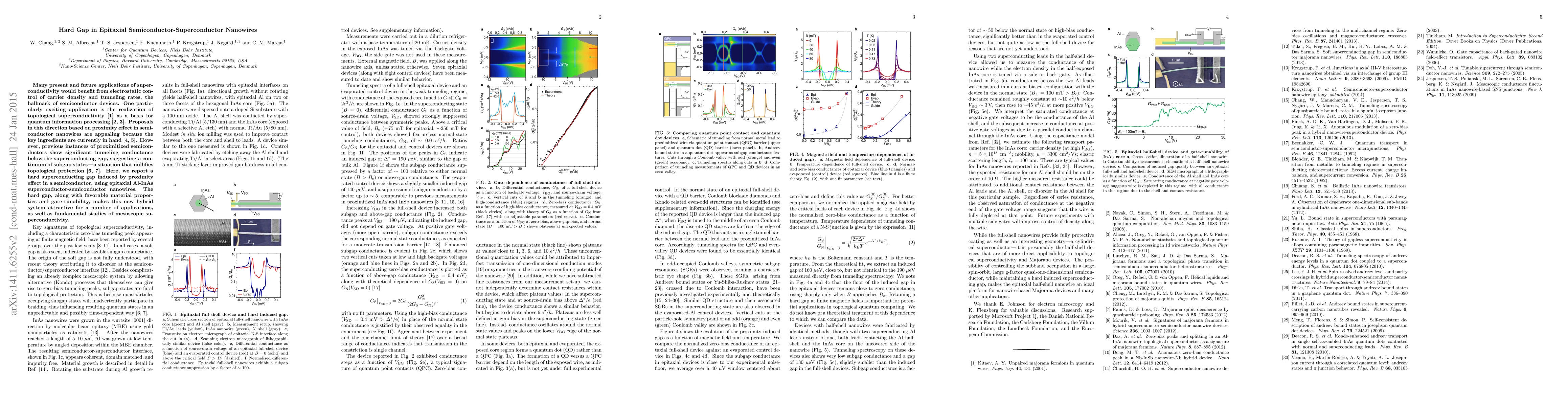
Many present and future applications of superconductivity would benefit from electrostatic control of carrier density and tunneling rates, the hallmark of semiconductor devices. One particularly exciting application is the realization of topological superconductivity as a basis for quantum information processing. Proposals in this direction based on proximity effect in semiconductor nanowires are appealing because the key ingredients are currently in hand. However, previous instances of proximitized semiconductors show significant tunneling conductance below the superconducting gap, suggesting a continuum of subgap states---a situation that nullifies topological protection. Here, we report a hard superconducting gap induced by proximity effect in a semiconductor, using epitaxial Al-InAs superconductor-semiconductor nanowires. The hard gap, along with favorable material properties and gate-tunability, makes this new hybrid system attractive for a number of applications, as well as fundamental studies of mesoscopic superconductivity.

Key Findings, in focus

Seven facets of this paper, analysed and brought into focus by AI.

AI-generated · verify against source Generated Sep 07, 2025
In focus · one-line synthesis

This research is important for applications such as topological superconductivity and Majorana devices.

01
MethodologyHow they did it

The research used epitaxial Al-InAs superconductor-semiconductor nanowires with gate-tunability to control carrier density and tunneling rates.

02
ResultsWhat they found
  • A hard gap was induced by proximity effect in the semiconductor
  • Favorable material properties and gate-tunability were observed
  • The device showed a saturation of conductance at negative gate voltages
03
SignificanceWhy it matters

This research is important for applications such as topological superconductivity and Majorana devices.

04
Technical ContributionsWhat's new technically

The research introduced a hard gap in epitaxial semiconductor-superconductor nanowires using proximity effect.

05
NoveltyWhat sets it apart

This work is novel because it demonstrates a hard gap in a semiconductor-superconductor hybrid system, which is a key ingredient for topological superconductivity.

06
LimitationsWhat to be cautious about
  • Previous instances of proximitized semiconductors show significant tunneling conductance below the superconducting gap
  • The device showed a high resistance due to contact resistance
07
Future WorkWhere it goes next
  • Improving control over density along the wire
  • Investigating the properties of the Al shell and InAs core
  • Exploring the potential applications of this device in topological superconductivity

Impact

36
References
3
Influential

Paper Details

Paper ID: 1411.6255
Journal: Nature Nanotechnology 10, 232 (2015)
License: http://arxiv.org/licenses/nonexclusive-distrib/1.0/
Comments: Combined text and supplementary information, Nature Nanotechnology (2015)
Report No: NBI QDEV 2014
Categories:
cond-mat.mes-hall cond-mat.mtrl-sci cond-mat.supr-con

How to Cite This Paper

Reference manager: RIS EndNote

Key Terms

semiconductor (0.306)
superconductivity (0.269)
nanowires (0.249)
proximity (0.230)
tunneling (0.216)
gap (0.193)
superconducting (0.191)
hard (0.177)

Citation Network

Current paper (gray), citations (green), references (blue)

Display is limited for performance on very large graphs.

Current Paper
Citations
References
Click to view


Discussion 0

This website uses cookies to ensure you get the best experience. Learn more