Hard superconducting gap in PbTe nanowires
Publication
Metrics
AI Quick Summary
This study reports the first observation of a hard superconducting gap in PbTe nanowires coupled to Pb, essential for quantum devices like Majorana zero modes. The observed gap size is around 1 meV, with a transparency of the superconductor-semiconductor interface of approximately 0.96.
Paper Preview
Abstract
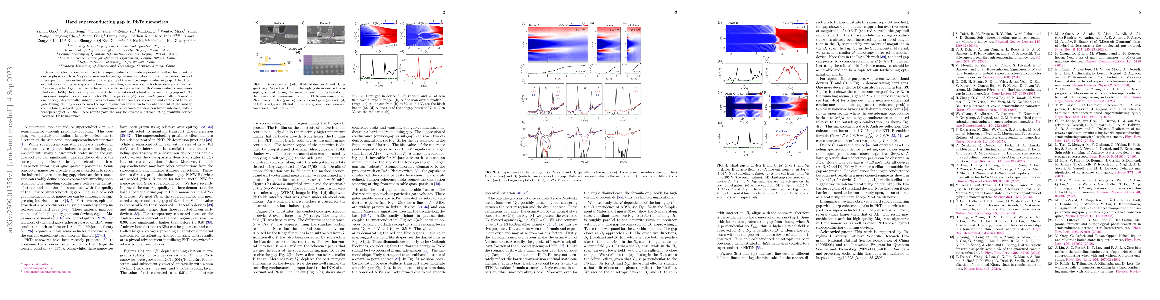
Semiconductor nanowires coupled to a superconductor provide a powerful testbed for quantum device physics such as Majorana zero modes and gate-tunable hybrid qubits. The performance of these quantum devices heavily relies on the quality of the induced superconducting gap. A hard gap, evident as vanishing subgap conductance in tunneling spectroscopy, is both necessary and desired. Previously, a hard gap has been achieved and extensively studied in III-V semiconductor nanowires (InAs and InSb). In this study, we present the observation of a hard superconducting gap in PbTe nanowires coupled to a superconductor Pb. The gap size ($\Delta$) is $\sim$ 1 meV (maximally 1.3 meV in one device). Additionally, subgap Andreev bound states can also be created and controlled through gate tuning. Tuning a device into the open regime can reveal Andreev enhancement of the subgap conductance, suggesting a remarkable transparent superconductor-semiconductor interface, with a transparency of $\sim$ 0.96. These results pave the way for diverse superconducting quantum devices based on PbTe nanowires.
AI Key Findings
Get AI-generated insights about this paper's methodology, results, significance, and more — seven facets brought into focus.
Impact
Paper Details
Authors
PDF Preview
Key Terms
Citation Network
Current paper (gray), citations (green), references (blue)
Display is limited for performance on very large graphs.
Discussion 0