Imaging interstitial atoms with multislice electron ptychography
Publication
Metrics
AI Quick Summary
This study demonstrates the capability of multislice electron ptychography to detect and locate single interstitial impurity atoms in three dimensions within complex garnet oxide heterostructures with sub-Ångstrom lateral and less than 2.7 nm depth resolution, offering a new method for characterizing atomic-scale defects and quantum sensors.
Paper Preview
Abstract
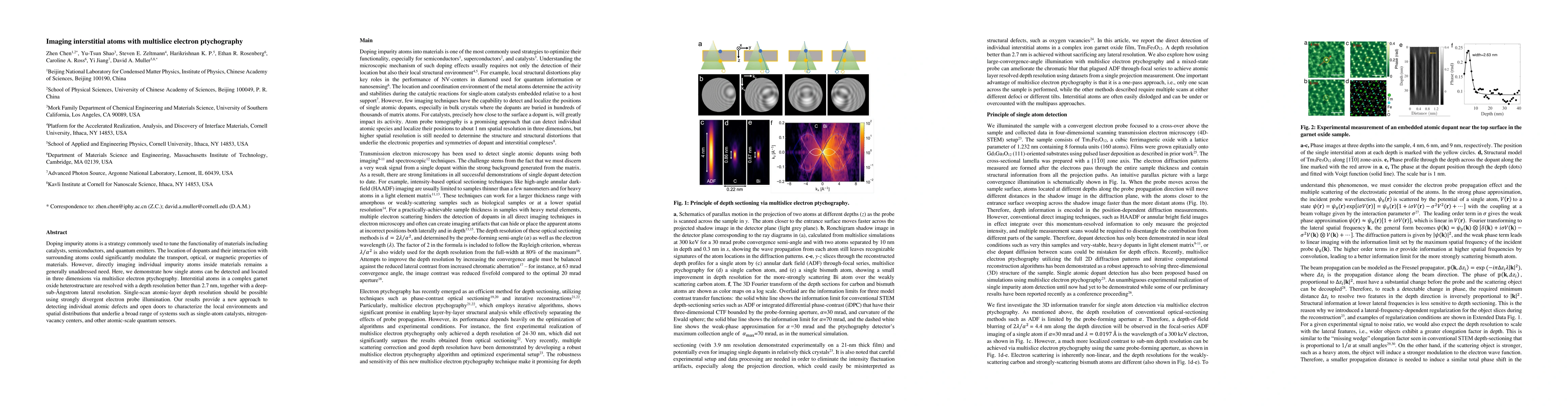
Doping impurity atoms is a strategy commonly used to tune the functionality of materials including catalysts, semiconductors, and quantum emitters. The location of dopants and their interaction with surrounding atoms could significantly modulate the transport, optical, or magnetic properties of materials. However, directly imaging individual impurity atoms inside materials remains a generally unaddressed need. Here, we demonstrate how single atoms can be detected and located in three dimensions via multislice electron ptychography.Interstitial atoms in a complex garnet oxide heterostructure are resolved with a depth resolution better than 2.7 nm, together with a deep-sub-{\AA}ngstrom lateral resolution. Single-scan atomic-layer depth resolution should be possible using strongly divergent electron probe illumination. Our results provide a new approach to detecting individual atomic defects and open doors to characterize the local environments and spatial distributions that underlie a broad range of systems such as single-atom catalysts, nitrogen-vacancy centers, and other atomic-scale quantum sensors.
AI Key Findings
Get AI-generated insights about this paper's methodology, results, significance, and more — seven facets brought into focus.
Impact
Paper Details
Authors
PDF Preview
Citation Network
Current paper (gray), citations (green), references (blue)
Display is limited for performance on very large graphs.
Discussion 0