Summary
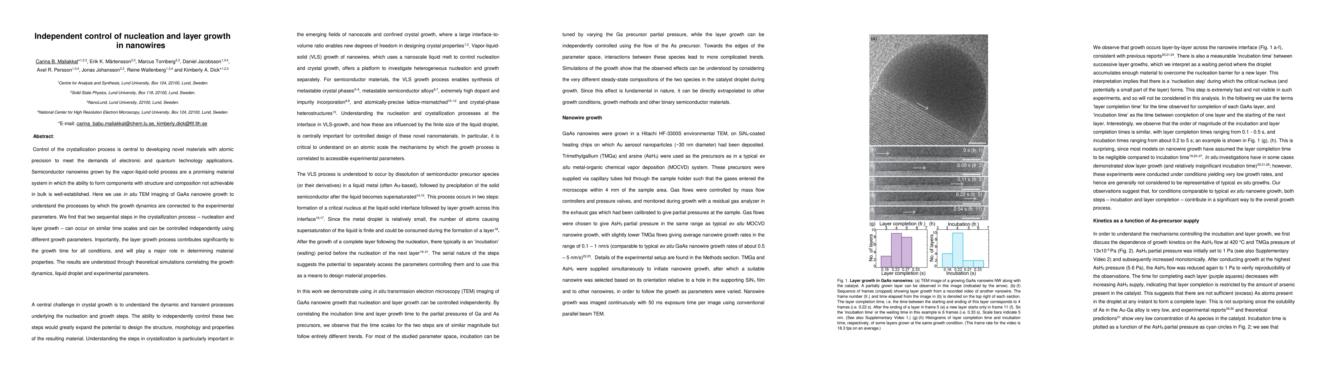
Control of the crystallization process is central to developing novel materials with atomic precision to meet the demands of electronic and quantum technology applications. Semiconductor nanowires grown by the vapor-liquid-solid process are a promising material system in which the ability to form components with structure and composition not achievable in bulk is well-established. Here we use in situ TEM imaging of GaAs nanowire growth to understand the processes by which the growth dynamics are connected to the experimental parameters. We find that two sequential steps in the crystallization process - nucleation and layer growth - can occur on similar time scales and can be controlled independently using different growth parameters. Importantly, the layer growth process contributes significantly to the growth time for all conditions, and will play a major role in determining material properties. The results are understood through theoretical simulations correlating the growth dynamics, liquid droplet and experimental parameters.
AI Key Findings
Get AI-generated insights about this paper's methodology, results, and significance.
Paper Details
PDF Preview
Key Terms
Citation Network
Current paper (gray), citations (green), references (blue)
Display is limited for performance on very large graphs.
Similar Papers
Found 4 papersZrN nucleation layer provides backside ohmic contact to MBE-grown GaN nanowires
Stanislav Tiagulskyi, Roman Yatskiv, Marta Sobanka et al.
PAMBE growth of GaN nanowires on metallic ZrN buffers -- a critical impact of ZrN layer thickness on the growth temperature
Karol Olszewski, Zbigniew R. Zytkiewicz, Aleksandra Wierzbicka et al.
Spontaneous nucleation and growth of GaN nanowires: Fundamental role of crystal polarity
Xiang Kong, Oliver Brandt, Sergio Fernández-Garrido et al.
| Title | Authors | Year | Actions |
|---|
Comments (0)