Large-Area Deterministic Stamping of 2D Materials on Arbitrarily Patterned Surfaces
Publication
Metrics
Paper Preview
Abstract
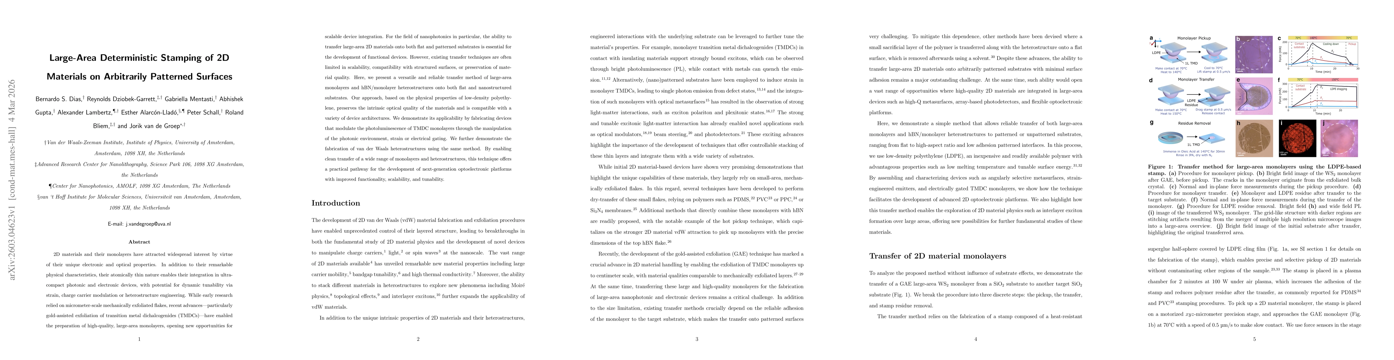
2D materials and their monolayers have attracted widespread interest by virtue of their unique electronic and optical properties. In addition to their remarkable physical characteristics, their atomically thin nature enables their integration in ultra-compact photonic and electronic devices, with potential for dynamic tunability via strain, charge carrier modulation or heterostructure engineering. While early research relied on micrometer-scale mechanically exfoliated flakes, recent advances, particularly gold-assisted exfoliation of transition metal dichalcogenides (TMDCs), have enabled the preparation of high-quality, large-area monolayers, opening new opportunities for scalable device integration. For the field of nanophotonics in particular, the ability to transfer large-area 2D materials onto both flat and patterned substrates is essential for the development of functional devices. However, existing transfer techniques are often limited in scalability, and compatibility with structured surfaces. Here, we present a versatile and reliable transfer method of large-area monolayers and hBN/monolayer heterostructures onto both flat and nanostructured substrates. Our approach, based on the physical properties of low-density polyethylene, preserves the intrinsic optical quality of the materials and is compatible with a variety of device architectures. We demonstrate its applicability by fabricating devices that modulate the photoluminescence of TMDC monolayers through the manipulation of the photonic environment, strain or electrical gating. We further demonstrate the fabrication of van der Waals heterostructures using the same method. By enabling clean transfer of a wide range of monolayers and heterostructures, this technique offers a practical pathway for the development of next-generation optoelectronic platforms with improved functionality, scalability, and tunability.
AI Key Findings
Get AI-generated insights about this paper's methodology, results, significance, and more — seven facets brought into focus.
Discussion 0