Publication
Metrics
AI Quick Summary
This paper presents a laser-thinning technique to controllably reduce multilayer MoS2 to single-layer semiconductors, achieving arbitrary shapes and patterns with high precision. The resulting single-layer MoS2 maintains optical and electronic properties similar to those of pristine exfoliated layers, offering potential for advanced electronic and optoelectronic applications.
Paper Preview
Abstract
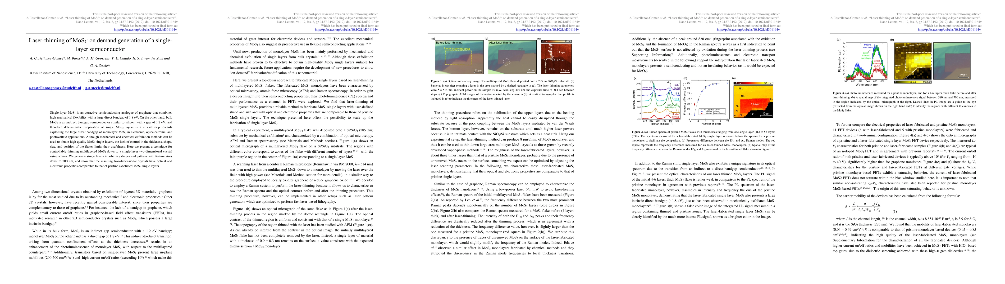
Single-layer MoS2 is an attractive semiconducting analogue of graphene that combines high mechanical flexibility with a large direct bandgap of 1.8 eV. On the other hand, bulk MoS2 is an indirect bandgap semiconductor similar to silicon, with a gap of 1.2 eV, and therefore deterministic preparation of single MoS2 layers is a crucial step towards exploiting the large direct bandgap of monolayer MoS2 in electronic, optoelectronic, and photovoltaic applications. Although mechanical and chemical exfoliation methods can be used to obtain high quality MoS2 single-layers, the lack of control in the thickness, shape, size, and position of the flakes limits their usefulness. Here we present a technique for controllably thinning multilayered MoS2 down to a single-layer two-dimensional crystal using a laser. We generate single layers in arbitrary shapes and patterns with feature sizes down to 200 nm, and show that the resulting two-dimensional crystals have optical and electronic properties comparable to that of pristine exfoliated MoS2 single layers.
AI Key Findings
Get AI-generated insights about this paper's methodology, results, significance, and more — seven facets brought into focus.
Impact
Paper Details
PDF Preview
Key Terms
Citation Network
Current paper (gray), citations (green), references (blue)
Display is limited for performance on very large graphs.
Discussion 0