Lateral electrodeposition of MoS2 semiconductor over an insulator
Publication
Metrics
AI Quick Summary
This paper demonstrates a novel electrochemical deposition technique for laterally growing MoS2 semiconductor films over insulating surfaces, achieving high anisotropy and confirming their semiconducting properties for photodetection applications. The method enables scalable, site-selective production of 2D transition metal dichalcogenides for advanced optoelectronic devices.
Paper Preview
Abstract
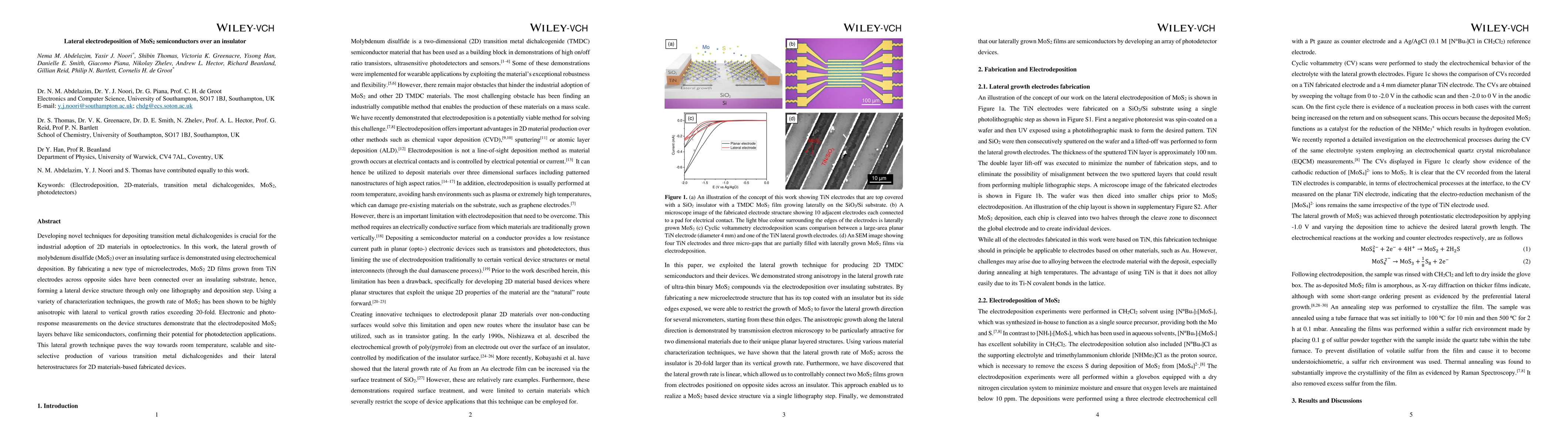
Developing novel techniques for depositing transition metal dichalcogenides is crucial for the industrial adoption of 2D materials in optoelectronics. In this work, the lateral growth of molybdenum disulfide (MoS2) over an insulating surface is demonstrated using electrochemical deposition. By fabricating a new type of microelectrodes, MoS2 2D films grown from TiN electrodes across opposite sides have been connected over an insulating substrate, hence, forming a lateral device structure through only one lithography and deposition step. Using a variety of characterization techniques, the growth rate of MoS2 has been shown to be highly anisotropic with lateral to vertical growth ratios exceeding 20-fold. Electronic and photo-response measurements on the device structures demonstrate that the electrodeposited MoS2 layers behave like semiconductors, confirming their potential for photodetection applications. This lateral growth technique paves the way towards room temperature, scalable and site-selective production of various transition metal dichalcogenides and their lateral heterostructures for 2D materials-based fabricated devices.
AI Key Findings
Get AI-generated insights about this paper's methodology, results, significance, and more — seven facets brought into focus.
Impact
Paper Details
Authors
PDF Preview
Key Terms
Citation Network
Current paper (gray), citations (green), references (blue)
Display is limited for performance on very large graphs.
Discussion 0