Quick Summary:

This paper presents a method for the deterministic localisation of hexagonal boron nitride (hBN) colour centres using patterned dielectric layers on graphene, achieved via atomic layer deposition. The approach maintains colour centre emission by preventing charge transfer, enabling scalable device applications such as spin qubits and quantum sensors.

Summary

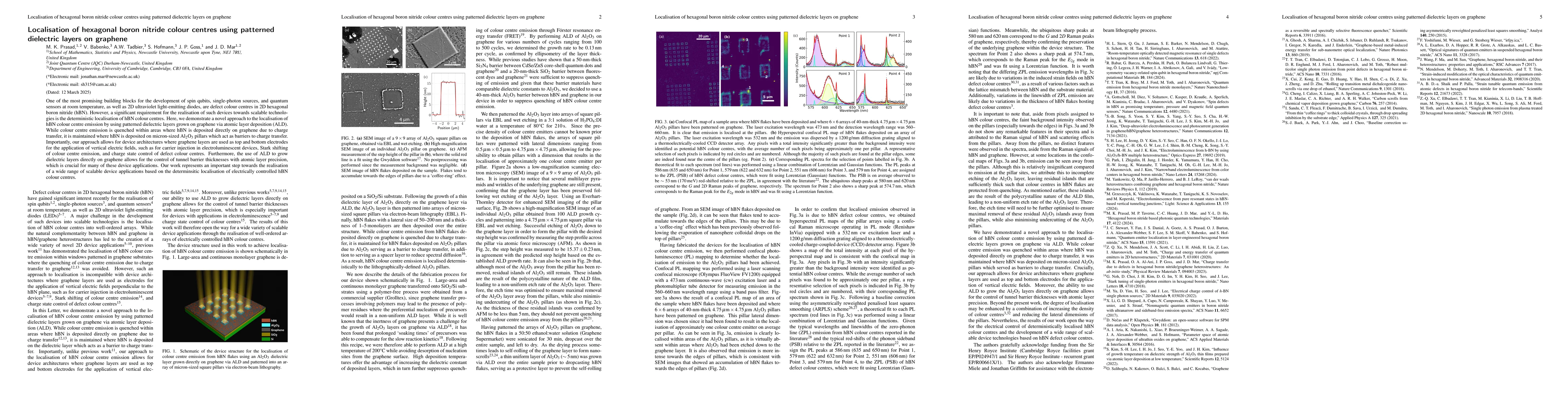
One of the most promising building blocks for the development of spin qubits, single-photon sources, and quantum sensors at room temperature, as well as 2D ultraviolet light-emitting diodes, are defect colour centres in 2D hexagonal boron nitride (hBN). However, a significant requirement for the realisation of such devices towards scalable technologies is the deterministic localisation of hBN colour centres. Here, we demonstrate a novel approach to the localisation of hBN colour centre emission by using patterned dielectric layers grown on graphene via atomic layer deposition (ALD). While colour centre emission is quenched within areas where hBN is deposited directly on graphene due to charge transfer, it is maintained where hBN is deposited on micron-sized Al2O3 pillars which act as barriers to charge transfer. Importantly, our approach allows for device architectures where graphene layers are used as top and bottom electrodes for the application of vertical electric fields, such as for carrier injection in electroluminescent devices, Stark shifting of colour centre emission, and charge state control of defect colour centres. Furthermore, the use of ALD to grow dielectric layers directly on graphene allows for the control of tunnel barrier thicknesses with atomic layer precision, which is crucial for many of these device applications. Our work represents an important step towards the realisation of a wide range of scalable device applications based on the determinsitic localisation of electrically controlled hBN colour centres

AI Key Findings

Generated Jun 10, 2025

Methodology

The research utilizes atomic layer deposition (ALD) to grow dielectric layers of Al2O3 on graphene, followed by patterning into micron-sized square pillars via electron-beam lithography (EBL) and wet etching. hBN flakes are then deposited over the structure, leading to localised colour centre emission at the pillars due to Al2O3 acting as a barrier to charge transfer.

Key Results

  • Demonstrated localisation of hBN colour centres using patterned dielectric layers on graphene.
  • Maintained colour centre emission on Al2O3 pillars while quenching on direct hBN-graphene contact.

Significance

This work represents a significant step towards realising scalable device applications based on deterministic localisation of electrically controlled hBN colour centres, which are promising for spin qubits, single-photon sources, quantum sensors, and 2D UV light-emitting diodes.

Technical Contribution

Novel approach to localising hBN colour centres using patterned dielectric layers on graphene via ALD, enabling the use of graphene as top and bottom electrodes for vertical electric fields.

Novelty

The use of ALD for growing dielectric layers directly on graphene with atomic layer precision for controlling tunnel barrier thicknesses is a key differentiator from previous methods.

Limitations

  • The paper does not discuss the scalability of the fabrication process for large-area devices.
  • Potential impact of residual Al2O3 islands on colour centre emission away from pillars is not fully addressed.

Future Work

  • Explore the scalability of the fabrication process for larger device architectures.
  • Investigate methods to further optimise etching to minimise residual Al2O3 islands.

Paper Details

PDF Preview

Download PDF

Key Terms

No key terms available for this paper.

Citation Network

Current paper (gray), citations (green), references (blue)

Current Paper
Citations
References
Click to view

No citations found for this paper.

Comments (0)

This website uses cookies to ensure you get the best experience. Learn more