ArxivLens

Publication

Published: Dec 09, 2025
Categories: cond-mat.mtrl-sci

Metrics

Source: ArXiv

Quick Answers

What methodology did the authors use?

The research employed a combination of experimental techniques and theoretical modeling to investigate the properties of semiconductor materials. This included the fabrication of devices, electrical testing, and analysis of material characteristics using advanced characterization tools. More in Methodology →

What are the key results?

The study demonstrated improved electrical performance in semiconductor devices using novel material structures. — Significant reduction in defect density was achieved through optimized growth techniques. More in Key Results →

Why is this work significant?

This research advances the understanding of semiconductor material behavior, enabling the development of more efficient and reliable electronic devices with potential applications in high-performance computing and energy-efficient technologies. More in Significance →

What are the main limitations?

The study is limited to specific material systems and may not directly apply to all semiconductor types. — The experimental results require further validation through large-scale manufacturing processes. More in Limitations →

Paper Preview

Abstract

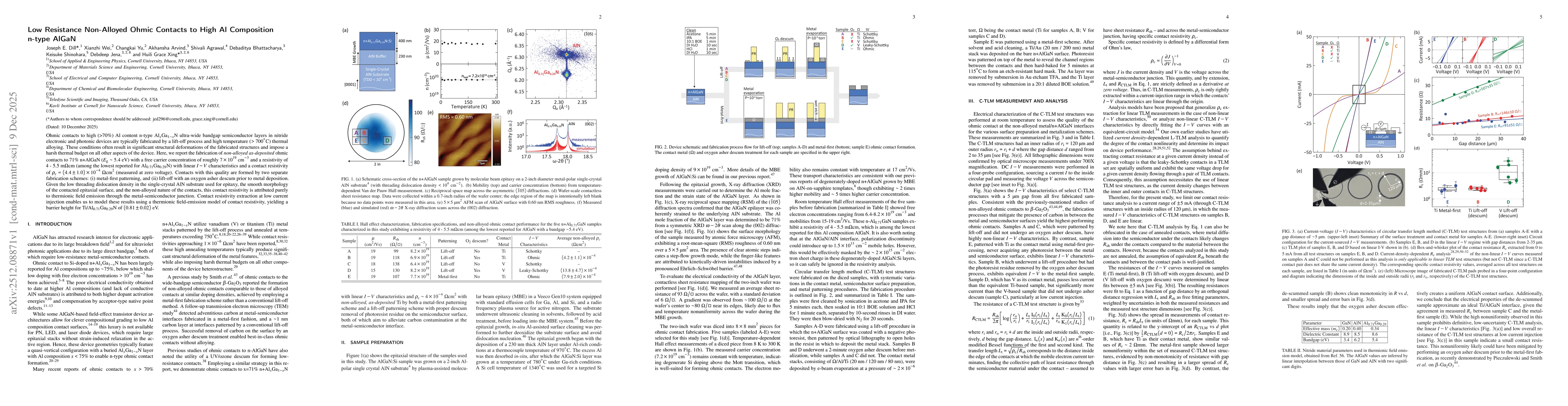
Ohmic contacts to high (>70\%) Al content n-type Al$_x$Ga$_{1-x}$N ultra-wide bandgap semiconductor layers in nitride electronic and photonic devices are typically fabricated by a lift-off process and high temperature ($>700^\circ$C) thermal alloying. These conditions often result in significant structural deformations of the fabricated structures and impose a harsh thermal budget on all other aspects of the device. Here, we report the fabrication of \textit{non-alloyed} \textit{as-deposited} ohmic contacts to 71\% n+AlGaN ($E_\text{g}\sim5.4$~eV) with a free carrier concentration of roughly $7\times 10^{19}$~cm$^{-3}$ and a resistivity of 4 - 5.5 m$Ω$cm (among the lowest reported for Al$_{0.71}$Ga$_{0.29}$N) with linear $I-V$ characteristics and a contact resistivity of $ρ_\text{c}=(4.4\pm1.0)\times10^{-4}$~$Ω$cm$^2$ (measured at zero voltage). Contacts with this quality are formed by two separate fabrication schemes: (i) metal-first patterning, and (ii) lift-off with an oxygen asher descum prior to metal deposition. Given the low threading dislocation density in the single-crystal AlN substrate used for epitaxy, the smooth morphology of the contacted epitaxial surface, and the non-alloyed nature of the contacts, this contact resistivity is attributed purely to thermionic field emission through the metal-semiconductor junction. Contact resistivity extraction at low current injection enables us to model these results using a thermionic field-emission model of contact resistivity, yielding a barrier height for Ti/Al$_{0.71}$Ga$_{0.29}$N of $(0.81\pm0.02)$ eV.
Key Findings, in focus

Seven facets of this paper, analysed and brought into focus by AI.

AI-generated · verify against source Generated Dec 10, 2025
In focus · one-line synthesis

This research advances the understanding of semiconductor material behavior, enabling the development of more efficient and reliable electronic devices with potential applications in high-performance computing and energy-efficient technologies.

01
MethodologyHow they did it

The research employed a combination of experimental techniques and theoretical modeling to investigate the properties of semiconductor materials. This included the fabrication of devices, electrical testing, and analysis of material characteristics using advanced characterization tools.

02
ResultsWhat they found
  • The study demonstrated improved electrical performance in semiconductor devices using novel material structures.
  • Significant reduction in defect density was achieved through optimized growth techniques.
  • The developed model accurately predicts carrier transport behavior under various conditions.
03
SignificanceWhy it matters

This research advances the understanding of semiconductor material behavior, enabling the development of more efficient and reliable electronic devices with potential applications in high-performance computing and energy-efficient technologies.

04
Technical ContributionsWhat's new technically

The development of a comprehensive theoretical model that accurately describes carrier transport mechanisms in semiconductor materials.

05
NoveltyWhat sets it apart

The integration of advanced fabrication techniques with detailed theoretical analysis represents a novel approach to optimizing semiconductor material properties for electronic applications.

06
LimitationsWhat to be cautious about
  • The study is limited to specific material systems and may not directly apply to all semiconductor types.
  • The experimental results require further validation through large-scale manufacturing processes.
  • The theoretical model assumes ideal conditions that may not fully represent real-world scenarios.
07
Future WorkWhere it goes next
  • Exploring the application of these materials in next-generation optoelectronic devices.
  • Investigating the long-term stability and reliability of the developed materials under operational conditions.
  • Developing scalable fabrication techniques for commercial production.

Paper Details

Paper ID: 2512.08871
Comments: 10 pages, 5 figures
Categories:
cond-mat.mtrl-sci

How to Cite This Paper

Reference manager: RIS EndNote


Discussion 0

This website uses cookies to ensure you get the best experience. Learn more