Material-specific high-resolution table-top extreme ultraviolet microscopy
Publication
Metrics
AI Quick Summary
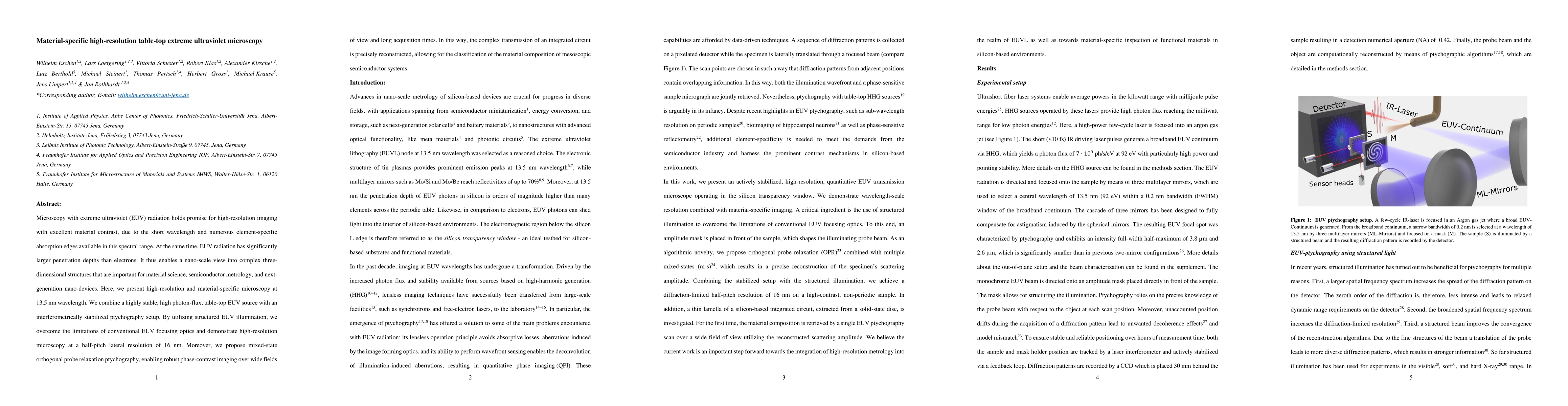
This paper presents high-resolution extreme ultraviolet (EUV) microscopy at 13.5 nm wavelength, combining a stable table-top EUV source with interferometrically stabilized ptychography to achieve a lateral resolution of 16 nm, enabling detailed material-specific imaging of semiconductor systems. The proposed mixed-state orthogonal probe relaxation ptychography method allows for robust phase-contrast imaging over large areas.
Paper Preview
Abstract
Microscopy with extreme ultraviolet (EUV) radiation holds promise for high-resolution imaging with excellent material contrast, due to the short wavelength and numerous element-specific absorption edges available in this spectral range. At the same time, EUV radiation has significantly larger penetration depths than electrons. It thus enables a nano-scale view into complex three-dimensional structures that are important for material science, semiconductor metrology, and next-generation nano-devices. Here, we present high-resolution and material-specific microscopy at 13.5 nm wavelength. We combine a highly stable, high photon-flux, table-top EUV source with an interferometrically stabilized ptychography setup. By utilizing structured EUV illumination, we overcome the limitations of conventional EUV focusing optics and demonstrate high-resolution microscopy at a half-pitch lateral resolution of 16 nm. Moreover, we propose mixed-state orthogonal probe relaxation ptychography, enabling robust phase-contrast imaging over wide fields of view and long acquisition times. In this way, the complex transmission of an integrated circuit is precisely reconstructed, allowing for the classification of the material composition of mesoscopic semiconductor systems.
AI Key Findings
Get AI-generated insights about this paper's methodology, results, significance, and more — seven facets brought into focus.
Impact
Paper Details
Authors
PDF Preview
Key Terms
Citation Network
Current paper (gray), citations (green), references (blue)
Display is limited for performance on very large graphs.
Discussion 0