Summary
Atomic-level imperfections play an increasingly critical role in nanophotonic device performance. However, it remains challenging to accurately characterize the sidewall roughness with sub-nanometer resolution and directly correlate this roughness with device performance. We have developed a method that allows us to measure the sidewall roughness of waveguides made of any material (including dielectrics) using the high resolution of atomic force microscopy. We illustrate this method by measuring state-of-the-art photonic devices made of silicon nitride. We compare the roughness of devices fabricated using both DUV photo-lithography and electron-beam lithography for two different etch processes. To correlate roughness with device performance we describe what we call a new Payne-Lacey Bending model, which adds a correction factor to the widely used Payne-Lacey model so that losses in resonators and waveguides with bends can be accurately predicted given the sidewall roughness, waveguide width and bending radii. Having a better way to measure roughness and use it to predict device performance can allow researchers and engineers to optimize fabrication for state-of-the-art photonics using many materials.
AI Key Findings
Get AI-generated insights about this paper's methodology, results, and significance.
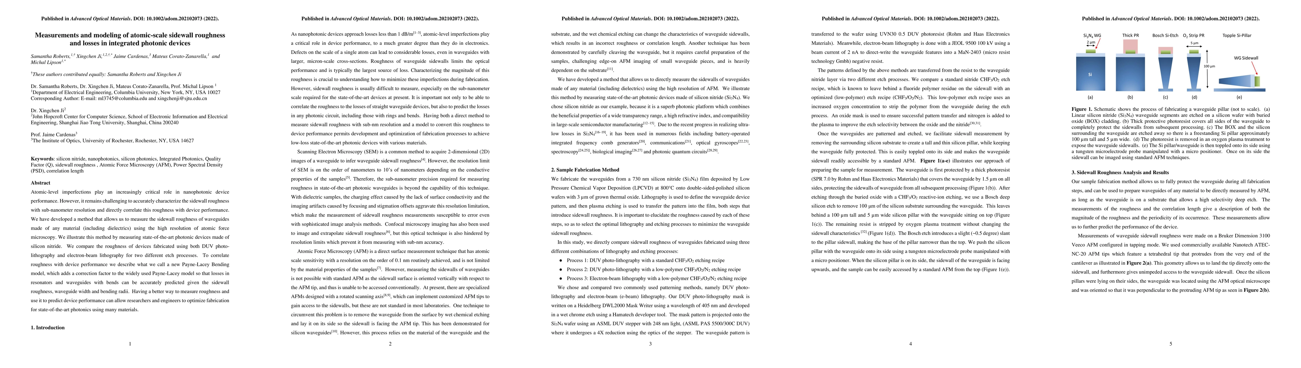
Paper Details
PDF Preview
Key Terms
Citation Network
Current paper (gray), citations (green), references (blue)
Display is limited for performance on very large graphs.
Similar Papers
Found 4 papersWafer-scale waveguide sidewall roughness scattering loss characterization by image processing
Zhenhuan Yi, Mohit Khurana, Sahar Delfan
Integrated Photonic Topology Optimization with Nonvertical Sidewall Profiles: Applications in Lithium Niobate and Silicon
Michael J. Probst, Stephen E. Ralph, Archana Kaushalram et al.
3D Atomic-Scale Metrology of Strain Relaxation and Roughness in Gate-All-Around (GAA) Transistors via Electron Ptychography
David A. Muller, Steven E. Zeltmann, Shake Karapetyan et al.
| Title | Authors | Year | Actions |
|---|
Comments (0)