Wafer-scale waveguide sidewall roughness scattering loss characterization by image processing
Publication
Metrics
AI Quick Summary
This research evaluates wafer-scale sidewall roughness in photonic integrated circuits (PICs) using high-resolution scanning electron microscope imaging and image processing, achieving a record lowest scattering loss of 0.075 dB/cm at 633 nm for fundamental transverse electric mode. The method correlates scattering loss to 2D image-based sidewall profiles and theoretical models, offering scalable insights for PIC fabrication.
Paper Preview
Abstract
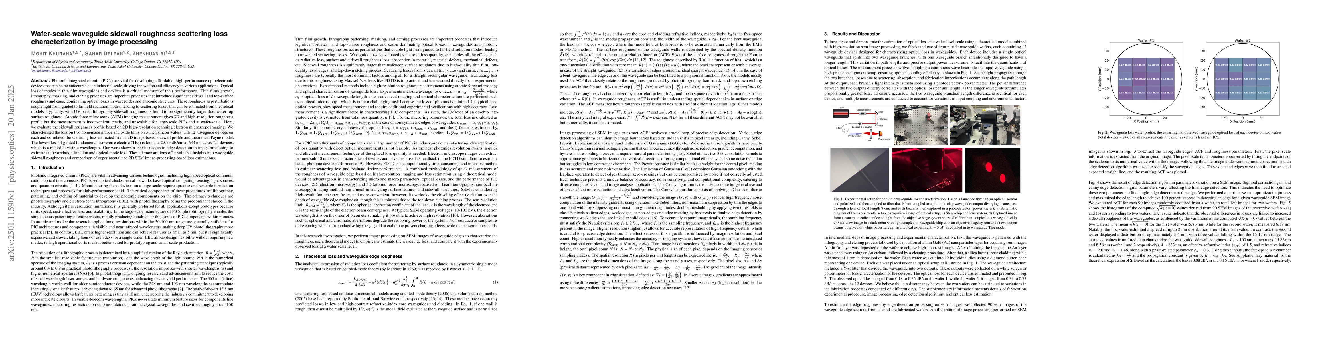
Photonic integrated circuits (PICs) are vital for developing affordable, high-performance optoelectronic devices that can be manufactured at an industrial scale, driving innovation and efficiency in various applications. Optical loss of modes in thin film waveguides and devices is a critical measure of their performance. Thin films growth, lithography, masking, and etching processes are imperfect processes that introduce significant sidewall and top-surface roughness and cause dominating optical losses in waveguides and photonic structures. These roughness as perturbations couple light from guided to far-field radiation modes, leading to scattering losses that can be estimated from theoretical models. Typically, with UV-based lithography sidewall roughness is found to be significantly larger than wafer-top surface roughness. Atomic force microscopy (AFM) imaging measurement gives 3D and high-resolution roughness profile but the measurement is inconvenient, costly, and unscalable for large-scale PICs and at wafer-scale. Here, we evaluate the sidewall roughness profile based on 2D high-resolution scanning electron microscope imaging. We characterized the loss on two homemade nitride and oxide films on 3-inch silicon wafers with 12 waveguide devices on each and co-related the scattering loss estimated from a 2D image-based sidewall profile and theoretical Payne model. The lowest loss of guided fundamental transverse electric (TE$_{0}$) is found at 0.075 dB/cm at 633 nm across 24 devices, which is a record at visible wavelength. Our work shows a 100% success in edge detection in image processing to estimate autocorrelation function and optical mode loss. These demonstrations offer valuable insights into waveguide sidewall roughness and comparison of experimental and 2D SEM image-processing-based loss estimations.
AI Key Findings
Get AI-generated insights about this paper's methodology, results, significance, and more — seven facets brought into focus.
Paper Details
Authors
PDF Preview
Related Papers
No references found for this paper.
Discussion 0