Quick Summary:

Researchers discovered that applying nano-indentation to a monolayer of MoS2 using an AFM tip reversibly reduces its tunneling resistance by up to 4 orders of magnitude, making it suitable for non-impacting nano-electro-mechanical switches.

Summary

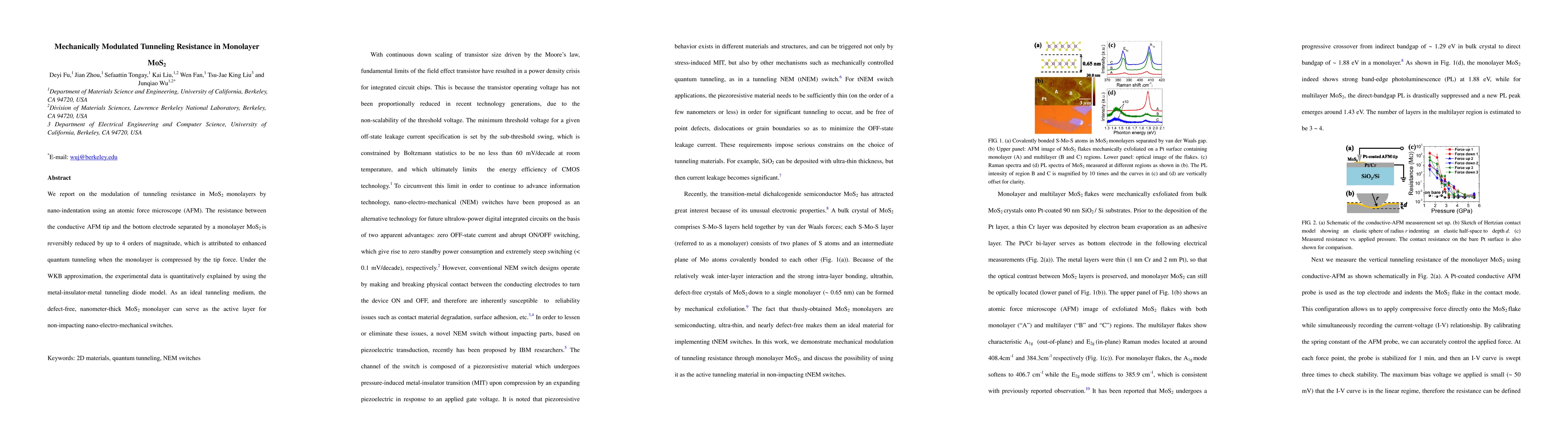
We report on the modulation of tunneling resistance in MoS2 monolayers by nano-indentation using an atomic force microscope (AFM). The resistance between the conductive AFM tip and the bottom electrode separated by a monolayer MoS2 is reversibly reduced by up to 4 orders of magnitude, which is attributed to enhanced quantum tunneling when the monolayer is compressed by the tip force. Under the WKB approximation, the experimental data is quantitatively explained by using the metal-insulator-metal tunneling diode model. As an ideal tunneling medium, the defect-free, nanometer-thick MoS2 monolayer can serve as the active layer for non-impacting nano-electro-mechanical switches.

AI Key Findings

Get AI-generated insights about this paper's methodology, results, and significance.

Paper Details

PDF Preview

Download PDF

Key Terms

tunneling (0.356)
monolayer (0.348)
tip (0.284)
nano (0.266)
resistance (0.254)
metal (0.212)
force (0.208)
compressed (0.159)
attributed (0.159)
defect (0.157)
insulator (0.151)
serve (0.148)
quantitatively (0.147)
separated (0.140)
modulation (0.139)
orders magnitude (0.139)
experimental data (0.136)
explained (0.134)
ideal (0.132)
mechanical (0.129)

Citation Network

Current paper (gray), citations (green), references (blue)

Current Paper
Citations
References
Click to view
Title Authors Year Actions
Unraveling the Interfacial Properties of Twisted Single-Crystal Au(111)/MoS2 Heterostructures: A Pathway to Robust Superlubricity.
Yuanpeng Yao, Yiming Song, Bozhao Wu, Sebastian Scherb, Shuyu Huang, A. Hinaut, T. Glatzel, Ernst Meyer, Ze Liu, Wengen Ouyang
2025
View Paper
Optimizing electrical AFM probing for 2D materials: The crucial role of tip-sample electrical interactions and back contact configurations
Md Ashiqur Rahman Laskar, Srijan Chakrabarti, Sakib Ahmed, S. A. Ghoreishi, Pinakapani Tummala, Valeri Afanas’Ev, Alessandro Molle, A. Lamperti, U. Celano
2025
View Paper
Low resistance electrical contacts to few-layered MoS2 by local pressurization
Y. Manzanares-Negro, Jiamin Quan, M. Rassekh, M. Moaied, Xiaoqin Li, P. Ares, J. Palacios, J. Gómez‐Herrero, C. Gómez-Navarro
2023
View Paper
High-pressure studies of atomically thin van der Waals materials
Luiz G. Pimenta Martins, R. Comin, M. J. Matos, M. Mazzoni, B. Neves, M. Yankowitz
2023
View Paper
Probing the uniaxial strain-dependent valley drift and Berry curvature in monolayer <mml:math xmlns:mml="http://www.w3.org/1998/Math/MathML"><mml:mrow><mml:msub><mml:mtext>MoSi</mml:mtext><mml:mn>2</mml:mn></mml:msub><mml:msub><mml:mtext>N</mml:mtext><mml:mn>4</mml:mn></mml:msub></mml:mrow></mml:ma
Sajjan Sheoran, Manjari Jain, Ruman Moulik, S. Bhattacharya
2023
View Paper
Transformation and reconstruction towards two-dimensional atomic laminates
Z. Du, Zongju Cheng, Qianchuan Zhao, Haiyan Wang, Qiang-juan Zhu, Hao-qi Chen, Xiao Chen, Bin Li, Shubin Yang
2023
View Paper
Mechanical Stress Modulation of Resistance in MoS2 Junctions.
Pradeep Chaudhary, Haidong Lu, Michael J. Loes, A. Lipatov, A. Sinitskii, A. Gruverman
2022
View Paper
Electromechanical Modulations in Transition Metal Dichalcogenide Nanosheets: Implications for Environmental Sensors
Mauricio V. Bessa, W. D. Freitas, N. P. Neme, L. G. P. Martins, A. P. Barboza, M. J. Matos, M. Mazzoni, B. Neves
2021
View Paper
Understanding Nanoscale Plasticity by Quantitative In Situ Conductive Nanoindentation
J. George, S. Mannepalli, Kiran Mangalampalli
2021
View Paper
Strain, Doping, and Electronic Transport of Large Area Monolayer MoS2 Exfoliated on Gold and Transferred to an Insulating Substrate
S. Panasci, E. Schilirò, G. Greco, M. Cannas, F. Gelardi, S. Agnello, F. Roccaforte, F. Giannazzo
2021
View Paper
Direct Optoelectronic Imaging of 2D Semiconductor-3D Metal Buried Interfaces.
Kiyoung Jo, Pawan Kumar, J. Orr, S. B. Anantharaman, J. Miao, M. Motala, Arkamita Bandyopadhyay, K. Kisslinger, C. Muratore, V. Shenoy, E. Stach, N. Glavin, Deep Jariwala
2021
View Paper
Recent Advances in Strain-Induced Piezoelectric and Piezoresistive Effect-Engineered 2D Semiconductors for Adaptive Electronics and Optoelectronics
Feng Li, Tao Shen, Cong Wang, Yupeng Zhang, J. Qi, Han Zhang
2020
View Paper
Nonvolatile resistance switching in monolayer transition metal dichalcogenides: an explanation
C. Mihai, A. Velea, F. Sava
2019
View Paper
Valley drift and valley current modulation in strained monolayer MoS2
Nityasagar Jena, Dimple, Raihan Ahammed, Ashima Rawat, M. Mohanta, Abir De Sarkar
2019
View Paper
Inter-cluster separation induced change in charge transport mechanism in Ni40Pd60 nanoclusters
S. Praveen, C. Bansal, D. Nagar
2019
View Paper
Strain engineering in functional 2-dimensional materials
Yufei Sun, Kai Liu
2019
View Paper
Universal Fermi-Level Pinning in Transition-Metal Dichalcogenides
K. Sotthewes, R. van Bremen, E. Dollekamp, T. Boulogne, Krystian Nowakowski, Daan Kas, H. Zandvliet, P. Bampoulis
2019
View Paper
Charge carrier injection and transport engineering in two-dimensional transition metal dichalcogenides
J. D. Durán Retamal, Dharmaraj Periyanagounder, Jr-jian Ke, M. Tsai, Jr-hau He
2018
View Paper
Interface Characterization and Control of 2D Materials and Heterostructures
Xiaolong Liu, M. Hersam
2018
View Paper
Force and light tuning vertical tunneling current in the atomic layered MoS2
Feng Li, Zhixing Lu, Yann-Wen Lan, Liying Jiao, Minxuan Xu, Xiaoyang Zhu, Xiankun Zhang, Hualin Wu, J. Qi
2018
View Paper
Hydrogen evolution enhancement of ultra-low loading, size-selected molybdenum sulfide nanoclusters by sulfur enrichment
D. Escalera‐López, Y. Niu, S. J. Park, M. Isaacs, K. Wilson, R. Palmer, N. V. Rees
2018
View Paper
Behavior of carrier transports and their sensitivity to solar irradiation for devices that use MoS2 that is directly deposited on Si using the chemical vapor method
Y. Lin, T. Su, S. Chen
2017
View Paper
Towards Universal Non-Volatile Resistance Switching in Non-metallic Monolayer Atomic Sheets
Ruijing Ge, Xiaohan Wu, Myungsoo Kim, H. Chou, S. Sonde, L. Tao, Jack C. Lee, D. Akinwande
2017
View Paper
Tunneling Current and Topographical Measurements of Semiconducting Structures Relevant for Electronic Applications using Atomic Force Microscopy
B. Schoenek
2017
View Paper
Defect Dominated Charge Transport and Fermi Level Pinning in MoS2/Metal Contacts
P. Bampoulis, R. van Bremen, Q. Yao, B. Poelsema, H. Zandvliet, K. Sotthewes
2017
View Paper
SiO2 substrate passivation effects on the temperature-dependent electrical properties of MoS2 prepared by the chemical vapor deposition method
Y. Lin, T. Su
2017
View Paper
Strain engineering of Schottky barriers in single- and few-layer MoS2 vertical devices
Jorge Quereda, J. J. Palacios, Nicolás Agräit, A. Castellanos-Gómez, G. Rubio‐Bollinger
2017
View Paper
Interface modification of MoS 2 /SiO 2 leading to conversion of conduction type of MoS 2
Y. Lin, T. Su
2016
View Paper
Investigations of vapour-phase deposited transition metal dichalcogenide films for future electronic applications
Riley Gatensby, T. Hallam, Kangho Lee, N. McEvoy, G. Duesberg
2016
View Paper
Fabrication of MoS2 Nanowire Arrays and Layered Structures via the Self‐Assembly of Block Copolymers
Atul Chaudhari, T. Ghoshal, M. Shaw, John O’Connell, R. Kelly, C. Glynn, C. O’Dwyer, J. Holmes, M. Morris
2016
View Paper
Directional dependent piezoelectric effect in CVD grown monolayer MoS2 for flexible piezoelectric nanogenerators
Sung Kyun Kim, Ravi Bhatia, Tae-ho Kim, Daehee Seol, Jung Ho Kim, Hyun Kim, Wanchul Seung, Yunseok Kim, Young Hee Lee, Sang‐Woo Kim
2016
View Paper
Effects of nitrogen plasma treatment on the electrical property and band structure of few-layer MoS2
T. Su, Y. Lin
2016
View Paper
Vibrational spectrum renormalization by enforced coupling across the van der Waals gap between MoS2 and WS2 monolayers
W. Fan, Xi Zhu, F. Ke, Yabin Chen, Kaichen Dong, J. Ji, Bin Chen, S. Tongay, J. Ager, Kai Liu, H. Su, Junqiao Wu
2015
View Paper
Enhanced photovoltaic performances of graphene/Si solar cells by insertion of a MoS₂ thin film.
Yuka Tsuboi, Feijiu Wang, D. Kozawa, K. Funahashi, S. Mouri, Y. Miyauchi, T. Takenobu, K. Matsuda
2015
View Paper
Multilayer MoS2 transistors enabled by a facile dry-transfer technique and thermal annealing
R. Yang, Xu-Qian Zheng, Zenghui Wang, Christopher J. Miller, P. Feng
2014
View Paper
Electrical breakdown of multilayer MoS2 field-effect transistors with thickness-dependent mobility.
R. Yang, Zenghui Wang, P. Feng
2014
View Paper
Schottky barrier heights for Au and Pd contacts to MoS2
Naveen Kaushik, Ankur Nipane, F. Basheer, Sudipta Dubey, S. Grover, M. Deshmukh, S. Lodha
2014
View Paper
Monolayer MoSe2 grown by chemical vapor deposition for fast photodetection.
Yung‐Huang Chang, Wenjing Zhang, Yihan Zhu, Yu Han, J. Pu, Jan-Kai Chang, W. Hsu, Jing-Kai Huang, Chang‐Lung Hsu, Ming-Hui Chiu, T. Takenobu, Henan Li, Chih‐I Wu, Wen‐Hao Chang, A. Wee, Lain‐Jong Li
2014
View Paper
Structure and electronic properties of in situ synthesized single-layer MoS2 on a gold surface.
Signe G Sørensen, Henrik G. Füchtbauer, A. Tuxen, A. Walton, J. Lauritsen
2014
View Paper
Pressure-induced semiconducting to metallic transition in multilayered molybdenum disulphide
A. Nayak, S. Bhattacharyya, Jie Zhu, Jin Liu, Xiang Wu, T. Pandey, C. Jin, A. Singh, D. Akinwande, Jung‐Fu Lin
2014
View Paper
Extreme sub-threshold swing in tunnelling relays
M. Abdelghany, T. Szkopek
2014
View Paper
Electrical and optoelectronic properties for devices that use MoS2 deposited on Si substrates with and without (NH4)2Sx treatment by chemical vapor deposition
T. Su, Chang-Lin Wu, Hsing-Cheng Chang, Y. Lin
2017
View Paper
Flexible IGZO Schottky diodes on paper
J. Kaczmarski, M. Borysiewicz, K. Piskorski, M. Wzorek, M. Kozubal, E. Kamińska
2017
View Paper
Fabrication of sub-10 nm lamellar structures by solvent vapour annealing of block copolymers
Atul Chaudhari
2015
View Paper

Comments (0)

This website uses cookies to ensure you get the best experience. Learn more