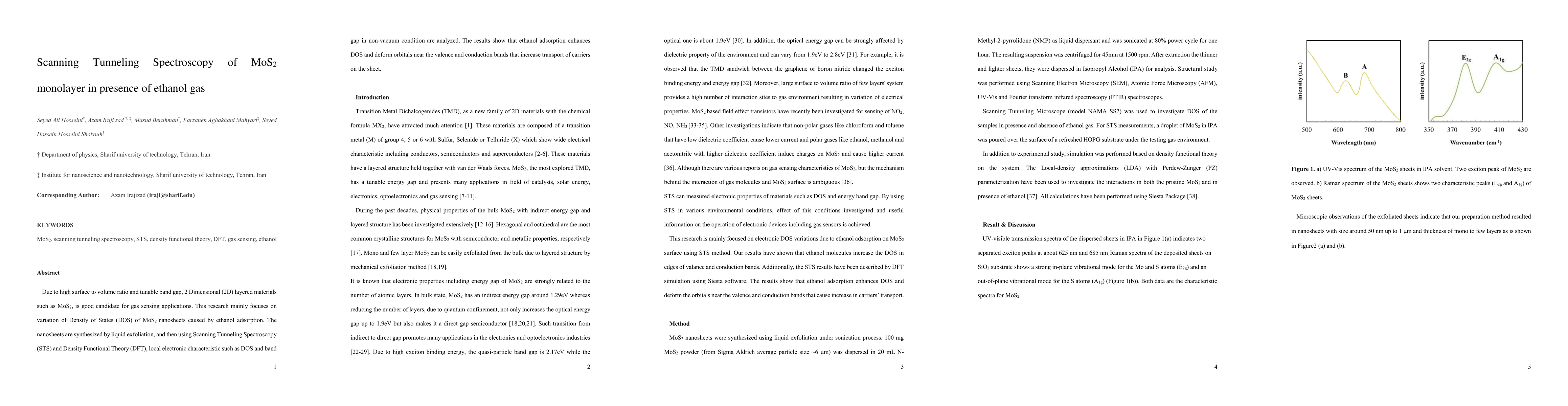
Coulomb engineering of the bandgap and excitons in two-dimensional materials
|
A. Raja, A. Chaves, Jaeeun Yu, Ghidewon Arefe, H. Hill, A. Rigosi, Timothy C. Berkelbach, P. Nagler, C. Schüller, T. Korn, C. Nuckolls, J. Hone, L. Brus, T. Heinz, D. Reichman, A. Chernikov
|
2017
|
View Paper
|
Electronic band gaps and exciton binding energies in monolayer M o x W 1 − x S 2 transition metal dichalcogenide alloys probed by scanning tunneling and optical spectroscopy
|
A. Rigosi, H. Hill, K. Rim, G. Flynn, T. Heinz
|
2016
|
View Paper
|
Monolayer MoS2 Bandgap Modulation by Dielectric Environments and Tunable Bandgap Transistors
|
Junga Ryou, Yong-Sung Kim, S. Kc, Kyeongjae Cho
|
2016
|
View Paper
|
Selective chemical vapor sensing with few-layer MoS2 thin-film transistors: Comparison with graphene devices
|
R. Samnakay, C. Jiang, S. Rumyantsev, M. Shur, A. Balandin
|
2014
|
View Paper
|
Bandgap, mid-gap states, and gating effects in MoS2.
|
Chih-Pin Lu, Guohong Li, J. Mao, Li-Min Wang, E. Andrei
|
2014
|
View Paper
|
Extraordinary sunlight absorption and one nanometer thick photovoltaics using two-dimensional monolayer materials.
|
M. Bernardi, M. Palummo, J. Grossman
|
2013
|
View Paper
|
Sensing behavior of atomically thin-layered MoS2 transistors.
|
D. Late, Yi Kai Huang, B. T. Liu, Jagaran Acharya, Jagaran Acharya, S. Shirodkar, Jiajun Luo, A. Yan, D. Charles, U. Waghmare, V. Dravid, C. Rao
|
2013
|
View Paper
|
High performance multilayer MoS2 transistors with scandium contacts.
|
Saptarshi Das, Hong-Yan Chen, A. Penumatcha, J. Appenzeller
|
2013
|
View Paper
|
High mobility ambipolar MoS2 field-effect transistors: Substrate and dielectric effects
|
W. Bao, Xinghan Cai, Dohun Kim, K. Sridhara, M. Fuhrer
|
2012
|
View Paper
|
High‐Detectivity Multilayer MoS2 Phototransistors with Spectral Response from Ultraviolet to Infrared
|
Woong Choi, M. Cho, A. Konar, Jong Hak Lee, G. Cha, S. Hong, Sangsig Kim, Jeongyong Kim, D. Jena, J. Joo, Sunkook Kim
|
2012
|
View Paper
|
Monolayer $\hbox{MoS}_{2}$ Transistors Beyond the Technology Road Map
|
K. Alam, R. Lake
|
2012
|
View Paper
|
Layered semiconductor molybdenum disulfide nanomembrane based Schottky-barrier solar cells.
|
M. Shanmugam, C. Durcan, Bin Yu
|
2012
|
View Paper
|
Electronics and optoelectronics of two-dimensional transition metal dichalcogenides.
|
Qing Hua Wang, K. Kalantar-zadeh, A. Kis, J. Coleman, M. Strano
|
2012
|
View Paper
|
Fabrication of flexible MoS2 thin-film transistor arrays for practical gas-sensing applications.
|
Qiyuan He, Zhiyuan Zeng, Z. Yin, Hai Li, Shixin Wu, Xiao Huang, Hua Zhang
|
2012
|
View Paper
|
Electron-hole transport and photovoltaic effect in gated MoS2 Schottky junctions
|
M. Fontana, Tristan Deppe, A. Boyd, M. Rinzan, A. Liu, M. Paranjape, P. Barbara
|
2012
|
View Paper
|
MoS₂ nanosheet phototransistors with thickness-modulated optical energy gap.
|
H. Lee, S. Min, Youn-Gyung Chang, Min Kyu Park, Taewook Nam, Hyungjun Kim, J. Kim, S. Ryu, S. Im
|
2012
|
View Paper
|
Stable, Single-Layer MX2 Transition-Metal Oxides and Dichalcogenides in a Honeycomb-Like Structure
|
C. Ataca, H. Sahin, S. Ciraci
|
2012
|
View Paper
|
Single-layer MoS2 phototransistors.
|
Z. Yin, Hai Li, Hong Li, Lin Jiang, Yumeng Shi, Yinghui Sun, Gang Lu, Qing Zhang, Xiaodong Chen, Hua Zhang
|
2012
|
View Paper
|
Fabrication of single- and multilayer MoS2 film-based field-effect transistors for sensing NO at room temperature.
|
Hai Li, Z. Yin, Qiyuan He, H. Li, Xiao Huang, Gang Lu, D. Fam, A. Tok, Qing Zhang, Hua Zhang
|
2012
|
View Paper
|
Photoluminescence from chemically exfoliated MoS2.
|
G. Eda, H. Yamaguchi, D. Voiry, T. Fujita, Mingwei Chen, M. Chhowalla
|
2011
|
View Paper
|
How good can monolayer MoS₂ transistors be?
|
Y. Yoon, K. Ganapathi, S. Salahuddin
|
2011
|
View Paper
|
On the origin of charge-density waves in select layered transition-metal dichalcogenides
|
K. Rossnagel
|
2011
|
View Paper
|
Single-layer MoS2 transistors.
|
B. Radisavljevic, A. Radenović, J. Brivio, V. Giacometti, A. Kis
|
2011
|
View Paper
|
MoS2 and WS2 analogues of graphene.
|
H. S. S. Ramakrishna Matte, A. Gomathi, Arun K. Manna, D. Late, R. Datta, S. Pati, C. Rao
|
2010
|
View Paper
|
Atomically thin MoS₂: a new direct-gap semiconductor.
|
K. Mak, Changgu Lee, J. Hone, J. Shan, T. Heinz
|
2010
|
View Paper
|
Band structure of MoS 2 , MoSe 2 , and α − MoTe 2 : Angle-resolved photoelectron spectroscopy and ab initio calculations
|
T. Boeker, R. Severin, A. Mueller, C. Janowitz, R. Manzke, D. Voß, P. Krüger, A. Mazur, J. Pollmann
|
2001
|
View Paper
|
The SIESTA method for ab initio order-N materials simulation
|
José M Soler, Emilio Artacho, Julian D Gale, Alberto García, Javier Junquera, Pablo Ordejón, Daniel Sánchez-Portal
|
2001
|
View Paper
|
Charge density wave, superconductivity, and anomalous metallic behavior in 2D transition metal dichalcogenides.
|
A. Neto
|
2000
|
View Paper
|
Atomic-scale structure of single-layer MoS2 nanoclusters
|
S. Helveg, J. Lauritsen, E. Lægsgaard, I. Stensgaard, J. Nørskov, B. Clausen, H. Topsøe, F. Besenbacher
|
2000
|
View Paper
|
Cluster Approach of Active Sites in an MoS2 Catalyst
|
P. Faye, E. Payen, D. Bougeard
|
1999
|
View Paper
|
Hydrodesulfurization activity of MoS2 catalysts modified by chemical exfoliation
|
M. D. Del Valle, J. Cruz-Reyes, M. Avalos-Borja, S. Fuentes
|
1998
|
View Paper
|
Electronic properties of low dimensional solids : the physics and chemistry of layer type transition metal dichalcogenides and their intercalate complexes
|
A. Yoffe
|
1990
|
View Paper
|
An examination of the formation and characteristics of charge-density waves in inorganic materials with special reference to the two- and one-dimensional transition-metal chalcogenides
|
R. Withers, J. Wilson
|
1986
|
View Paper
|
Band structure, intercalation, and interlayer interactions of transition-metal dichalcogenides: Ti S 2 and LiTi S 2
|
C. Umrigar, D. Ellis, Ding-sheng Wang, H. Krakauer, M. Posternak
|
1982
|
View Paper
|
Self-interaction correction to density-functional approximations for many-electron systems
|
J. Perdew, A. Zunger
|
1981
|
View Paper
|
Energy Bands for 2H-NbSe2 and 2H-MoS2
|
L. Mattheiss
|
1973
|
View Paper
|
Mobility of Charge Carriers in Semiconducting Layer Structures
|
R. Fivaz, E. Mooser
|
1967
|
View Paper
|
Single Crystals of MoS2 Several Molecular Layers Thick
|
R. Frindt
|
1966
|
View Paper
|
Infrared Absorption Spectra of Monohydric Alcohols
|
I. Doroshenko, V. Pogorelov, V. Šablinskas
|
2013
|
View Paper
|
Band structure of MoS2, MoSe2, and a-MoTe2: Angle-resolved photoelectron spectroscopy and ab initio calculations
|
T. Böker, R. Severin, C. Janowitz, R. Manzke, P. Krüger, A. Mazur, J. Pollmann
|
2001
|
View Paper
|
1T-MoS2, a new metallic modification of molybdenum disulfide
|
F. Wypych, R. Schöllhorn
|
1992
|
View Paper
|
Band structure of molybdenum(IV) sulfide and niobium(IV) sulfide," Physical Review Letters, vol
|
|
1973
|
|
Bloch states in edge of conduction band at K (a), (b) and Γ points (c), (d) in absence (a), (c) and in presence (b), (d) of one ethanol molecule
|
|
|
|
High Figure S6. (a) tunneling current in terms of voltage and (b) DOS in terms of voltage for MoS2
|
|
|
|
Comments (0)